
XC2VP40-7FG676C
| Part Description |
Virtex®-II Pro Field Programmable Gate Array (FPGA) IC 416 3538944 43632 676-BGA |
|---|---|
| Quantity | 1,054 Available (as of June 14, 2026) |
| Product Category | Field Programmable Gate Array (FPGA) |
|---|---|
| Manufacturer | AMD |
| Manufacturing Status | Obsolete |
| Manufacturer Standard Lead Time | Contact Us |
| Datasheet |
Specifications & Environmental
| Device Package | 676-FBGA (27x27) | Grade | Commercial | Operating Temperature | 0°C – 85°C | ||
|---|---|---|---|---|---|---|---|
| Package / Case | 676-BGA | Number of I/O | 416 | Voltage | 1.425 V - 1.575 V | ||
| Mounting Method | Surface Mount | RoHS Compliance | RoHS non-compliant | REACH Compliance | REACH Unaffected | ||
| Moisture Sensitivity Level | 2A (4 Weeks) | Number of LABs/CLBs | 4848 | Number of Logic Elements/Cells | 43632 | ||
| Number of Gates | N/A | ECCN | 3A991D | HTS Code | 8542.39.0001 | ||
| Qualification | N/A | Total RAM Bits | 3538944 |
Overview of XC2VP40-7FG676C – Virtex®-II Pro FPGA, 676-BGA, 416 I/O
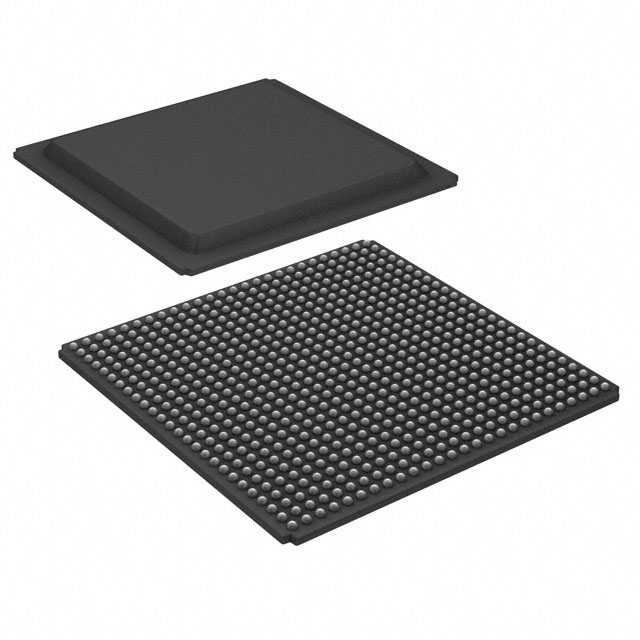
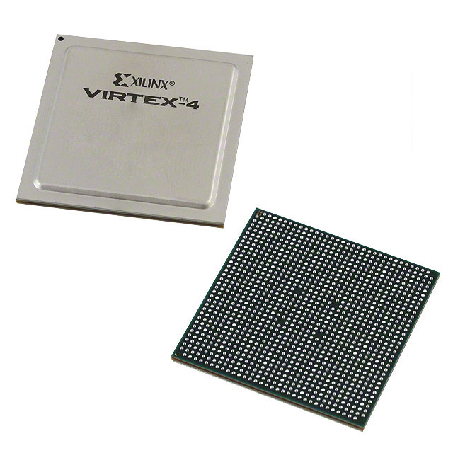
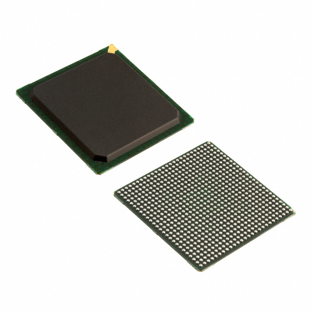
The XC2VP40-7FG676C is a Virtex®-II Pro platform field programmable gate array supplied in a 676-ball fine-pitch BGA (27 × 27 mm) surface-mount package. It delivers a high-density, configurable logic fabric with a large embedded memory complement and extensive I/O capability for complex system designs.
Built on the Virtex-II Pro family architecture, this device is appropriate for applications that require significant logic capacity, on-chip memory, and flexible I/O. Family-level features include embedded processor blocks and multi-gigabit transceiver options that support demanding communications and embedded processing use cases.
Key Features
- Logic Capacity — 43,632 logic elements provide substantial programmable logic for complex designs and high integration.
- Embedded Memory — Approximately 3.5 Mbits of on-chip RAM (3,538,944 bits) for buffering, frame storage, and local data handling.
- I/O Resources — 416 user I/O pins enable wide external interface support and high connectivity density.
- Package & Mounting — 676-FBGA (27 × 27 mm) package in a surface-mount form factor suited for compact PCBA layouts.
- Voltage & Power — Core supply range of 1.425 V to 1.575 V to match system power-rail requirements.
- Operating Range — Commercial grade specification with an operating temperature range of 0 °C to 85 °C.
- Family-Level Architecture — Virtex-II Pro platform features described in the product documentation include embedded processor blocks (PowerPC™ 405 cores), RocketIO™ multi-gigabit transceiver options, dedicated 18 × 18 multipliers, SelectRAM™ block RAM resources, and clock management circuitry.
- Regulatory — RoHS compliant.
Typical Applications
- Telecom and Datacom Systems — Suited for high-density logic and family-level multi-gigabit transceiver support for serial link and protocol processing functions.
- Embedded Processing — Use in systems that benefit from on-chip processor block integration and programmable logic to offload tasks or implement custom accelerators.
- High-Performance Networking — Large I/O count and substantial on-chip memory make this device applicable to packet processing, switching, and interface bridging.
- Signal Processing and Acceleration — Dedicated multiplier resources and abundant logic elements support arithmetic-heavy algorithms and custom datapaths.
Unique Advantages
- High Logic Density: 43,632 logic elements enable large-scale integration and consolidation of multiple functions onto a single device.
- Significant On-Chip Memory: Approximately 3.5 Mbits of embedded RAM reduce dependence on external memory for buffering and local storage.
- Robust I/O Capability: 416 I/O pins provide flexibility to interface with numerous peripherals and high-pin-count subsystems.
- Platform-Level Processing Options: Virtex-II Pro family support for embedded processor blocks allows combined hardware/software co-design on the same silicon.
- Commercial-Grade Reliability: Commercial temperature range and RoHS compliance support deployment in standard electronics environments while meeting regulatory expectations.
- Compact, Surface-Mount Packaging: 676-FBGA (27 × 27 mm) package supports dense PCB layouts and automated assembly processes.
Why Choose XC2VP40-7FG676C?
The XC2VP40-7FG676C positions itself as a high-capacity, Virtex-II Pro platform FPGA designed for applications that require a combination of abundant logic resources, embedded memory, and extensive I/O. Its platform-level features—documented in the Virtex-II Pro family specification—support designs that integrate processing blocks, high-speed serial links, and dedicated DSP resources.
This device is well suited to teams building complex communications, networking, or embedded-processor-based systems who need a commercially graded, RoHS-compliant FPGA in a compact 676-FBGA package with clearly defined power and thermal operating ranges.
Request a quote or submit an inquiry to receive pricing, availability, and ordering information for the XC2VP40-7FG676C.


Date Founded: 1969
Headquarters: Santa Clara, California, USA
Employees: 25,000+
Revenue: $22.68 Billion
Certifications and Memberships: ISO9001:2015, RoHS, REACH


