
XC2VP7-7FFG896C
| Part Description |
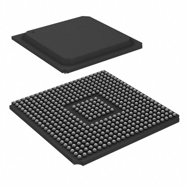
Virtex®-II Pro Field Programmable Gate Array (FPGA) IC 396 811008 11088 896-BBGA, FCBGA |
|---|---|
| Quantity | 583 Available (as of June 15, 2026) |

| Product Category | Field Programmable Gate Array (FPGA) |
|---|---|
| Manufacturer | AMD |
| Manufacturing Status | Obsolete |
| Manufacturer Standard Lead Time | Contact Us |
| Datasheet |
Specifications & Environmental
| Device Package | 896-FCBGA (31x31) | Grade | Commercial | Operating Temperature | 0°C – 85°C | ||
|---|---|---|---|---|---|---|---|
| Package / Case | 896-BBGA, FCBGA | Number of I/O | 396 | Voltage | 1.425 V - 1.575 V | ||
| Mounting Method | Surface Mount | RoHS Compliance | ROHS3 Compliant | REACH Compliance | REACH Unaffected | ||
| Moisture Sensitivity Level | 4 (72 Hours) | Number of LABs/CLBs | 1232 | Number of Logic Elements/Cells | 11088 | ||
| Number of Gates | N/A | ECCN | 3A991D | HTS Code | 8542.39.0001 | ||
| Qualification | N/A | Total RAM Bits | 811008 |
Overview of XC2VP7-7FFG896C – Virtex®-II Pro Field Programmable Gate Array, 896-FCBGA
The XC2VP7-7FFG896C is a commercial-grade Virtex®-II Pro platform FPGA from AMD, supplied in a 896-ball flip-chip BGA (896-FCBGA, 31×31) package. It provides a programmable fabric with substantial logic capacity, on-chip memory, and a high I/O count for board-level digital systems and complex interface implementations.
As a member of the Virtex®-II Pro family, this device aligns with the platform’s architectural focus on flexible logic resources, embedded memory hierarchy, and extensive I/O capability—making it suitable for applications that require dense custom logic, multiple interfaces, and on-chip buffering.
Key Features
- Logic Capacity – 11,088 logic elements for implementing custom digital functions, control logic and state machines.
- Configurable Logic Blocks – 1,232 CLB resources reported for mapped logic partitioning and parallel implementation.
- Embedded Memory – Approximately 0.81 Mbits of on-chip RAM (811,008 total RAM bits) for data buffering, FIFOs and small lookup tables.
- High I/O Count – 396 I/O pins to support complex interfacing and multiple parallel data paths.
- Power Supply – Core voltage range of 1.425 V to 1.575 V to match board-level power rails and regulator specifications.
- Package & Mounting – 896-FCBGA (31×31) flip-chip BGA, surface-mount package suitable for compact, high-density PCB layouts.
- Operating Range & Grade – Commercial grade operation from 0 °C to 85 °C for standard commercial applications.
- RoHS Compliant – Conforms to RoHS requirements for reduced hazardous substances.
- Virtex®-II Pro Platform Features – Part of a platform with documented IP core and reference support, high-performance clock management, SelectRAM™ memory hierarchy and dedicated multiplier resources (as described in the Virtex®-II Pro family documentation).
Typical Applications
- High-density I/O systems – The 396 I/O pins support multi-channel data interfaces, board-level protocol bridging and complex peripheral aggregation.
- Custom logic and prototyping – 11,088 logic elements enable implementation of bespoke control logic, state machines and prototype designs that require reprogrammability.
- Embedded buffering and packet processing – Approximately 0.81 Mbits of embedded RAM can be used for packet FIFOs, small caches or data buffering in communications and data-acquisition designs.
Unique Advantages
- High logic density: 11,088 logic elements provide the headroom to consolidate multiple functions into a single FPGA, reducing BOM and board complexity.
- Generous on-chip memory: Approximately 0.81 Mbits of embedded RAM supports buffering and temporary storage without external memory overhead.
- Extensive I/O resources: 396 I/Os make the device well-suited for designs with diverse, parallel or high-pin-count interfacing requirements.
- Compact, manufacturable package: The 896-FCBGA (31×31) surface-mount package enables dense PCB layouts while supporting reliable board assembly practices.
- Platform-level support: As part of the Virtex®-II Pro family, documentation highlights IP core and reference support and a robust architecture for modular design integration.
- Regulatory and grade clarity: Commercial temperature rating (0 °C to 85 °C) and RoHS compliance simplify sourcing and environmental compliance planning.
Why Choose XC2VP7-7FFG896C?
The XC2VP7-7FFG896C combines a substantial logic resource count, embedded RAM and a high I/O complement in a single, compact 896-FCBGA package—providing a practical platform for board-level designs that require programmable logic, on-chip buffering and dense interfacing. Its position within the Virtex®-II Pro family ensures designers can leverage the platform’s documented IP, clock management and memory hierarchy capabilities.
This device is ideal for engineering teams developing commercial embedded systems, communication interfaces and prototype platforms that demand reprogrammable logic, moderate on-chip memory and a high number of external I/Os, while conforming to standard commercial temperature and RoHS requirements.
If you would like pricing, availability or to request a formal quote for the XC2VP7-7FFG896C, please submit a quote request or contact our sales channel for a customized quotation and lead-time information.


Date Founded: 1969
Headquarters: Santa Clara, California, USA
Employees: 25,000+
Revenue: $22.68 Billion
Certifications and Memberships: ISO9001:2015, RoHS, REACH


