
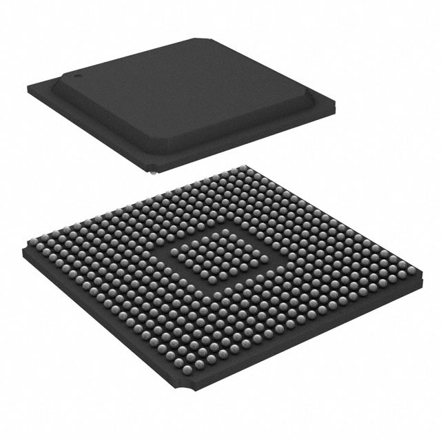
XC2VP70-5FF1517I
| Part Description |
Virtex®-II Pro Field Programmable Gate Array (FPGA) IC 964 6045696 74448 1517-BBGA, FCBGA |
|---|---|
| Quantity | 1,144 Available (as of June 15, 2026) |

| Product Category | Field Programmable Gate Array (FPGA) |
|---|---|
| Manufacturer | AMD |
| Manufacturing Status | Obsolete |
| Manufacturer Standard Lead Time | Contact Us |
| Datasheet |
Specifications & Environmental
| Device Package | 1517-FCBGA (40x40) | Grade | Industrial | Operating Temperature | -40°C – 100°C | ||
|---|---|---|---|---|---|---|---|
| Package / Case | 1517-BBGA, FCBGA | Number of I/O | 964 | Voltage | 1.425 V - 1.575 V | ||
| Mounting Method | Surface Mount | RoHS Compliance | RoHS non-compliant | REACH Compliance | REACH Unaffected | ||
| Moisture Sensitivity Level | 4 (72 Hours) | Number of LABs/CLBs | 8272 | Number of Logic Elements/Cells | 74448 | ||
| Number of Gates | N/A | ECCN | 3A001A7A | HTS Code | 8542.39.0001 | ||
| Qualification | N/A | Total RAM Bits | 6045696 |
Overview of XC2VP70-5FF1517I – Virtex®-II Pro Field Programmable Gate Array (FPGA) IC, 1517-BBGA FCBGA
The XC2VP70-5FF1517I is a Virtex®-II Pro family FPGA offered in a high-pin-count 1517-ball FCBGA package. It delivers large-scale programmable logic and system-level integration suitable for industrial applications that require dense logic, abundant I/O, and significant on-chip memory.
Built on the Virtex-II Pro platform, the device supports features identified for the family—such as embedded multi-gigabit transceivers and processor-block integration—while providing a wide operating temperature range, RoHS compliance, and a 1.425–1.575 V core supply window.
Key Features
- Logic Capacity 8,272 CLBs and 74,448 logic elements provide extensive programmable logic resources for complex designs and high integration.
- Embedded Memory Approximately 6.05 Mbits of on-chip RAM to support large buffering, lookup tables, and state storage without external memory.
- I/O Density 964 user I/O pins to enable broad connectivity and system integration from a single device.
- Family-Level Integration Virtex-II Pro family features include embedded RocketIO/RocketIO X multi-gigabit transceivers and up to two PowerPC RISC processor blocks for system-level integration (family capabilities per datasheet).
- Arithmetic & DSP Resources Dedicated 18-bit × 18-bit multiplier blocks and SelectRAM™ resources are included in the family architecture to accelerate arithmetic and DSP functions.
- Package & Mounting 1517-BBGA FCBGA (1517-FCBGA, 40×40) surface-mount package for high pin-count PCB implementations.
- Operating Conditions Industrial-grade operation from −40 °C to +100 °C and a core voltage supply range of 1.425–1.575 V.
- Compliance RoHS compliant for regulatory alignment in lead-free assemblies.
Typical Applications
- Telecommunications & Datacom: Use the family’s multi-gigabit transceiver capabilities and high I/O count for serial link endpoints, protocol bridging, and packet processing systems.
- Embedded Processing & Control: Integrate on-chip processor blocks and programmable logic to create consolidated control and signal-processing subsystems.
- High-Density Signal Processing: Leverage the large logic array, abundant multipliers, and on-chip RAM for DSP, filtering, and real-time data aggregation tasks.
- System Prototyping and Platform Development: High logic capacity and I/O make the device suitable for platform-level prototyping and integration of multiple subsystems on a single FPGA.
Unique Advantages
- Highly Integrated Platform: Family-level support for embedded transceivers and processor blocks reduces external component count and simplifies system architecture.
- Large On-Chip Resources: Tens of thousands of logic elements and approximately 6.05 Mbits of embedded memory allow complex functions and buffering without immediate need for external memory.
- Extensive I/O Connectivity: 964 I/O pins enable rich peripheral interfaces and high system connectivity from a single package.
- Industrial Temperature Range: Rated operation from −40 °C to +100 °C supports deployment in demanding environments.
- High-Pin FCBGA Package: The 1517-ball FCBGA (40×40) package supports compact, high-density PCB layouts for advanced designs.
- Regulatory Readiness: RoHS compliance helps with lead-free manufacturing workflows.
Why Choose XC2VP70-5FF1517I?
The XC2VP70-5FF1517I positions itself as a high-capacity, industrial-grade FPGA option within the Virtex-II Pro family, combining extensive logic resources, significant embedded memory, and very high I/O density in a single FCBGA package. It is suited to designers who need a platform-capable device for telecommunications, embedded processing, DSP, or platform prototyping where integration and on-chip resources reduce system complexity.
Choosing this device helps teams consolidate functions onto one FPGA, leverage family-level processor and transceiver capabilities, and maintain operation across a wide temperature range while adhering to RoHS requirements.
Request a quote or submit an inquiry to receive pricing, lead-time, and availability information for the XC2VP70-5FF1517I.


Date Founded: 1969
Headquarters: Santa Clara, California, USA
Employees: 25,000+
Revenue: $22.68 Billion
Certifications and Memberships: ISO9001:2015, RoHS, REACH


