
XC2VP7-7FFG672C
| Part Description |
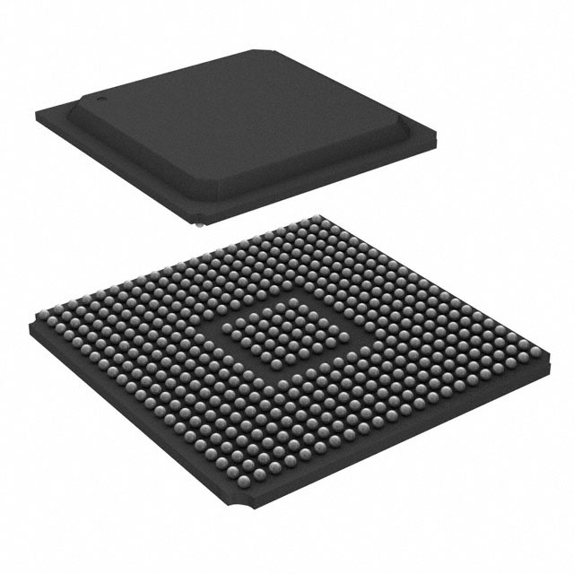
Virtex®-II Pro Field Programmable Gate Array (FPGA) IC 396 811008 11088 672-BBGA, FCBGA |
|---|---|
| Quantity | 1,062 Available (as of June 10, 2026) |

| Product Category | Field Programmable Gate Array (FPGA) |
|---|---|
| Manufacturer | AMD |
| Manufacturing Status | Obsolete |
| Manufacturer Standard Lead Time | Contact Us |
| Datasheet |
Specifications & Environmental
| Device Package | 672-FCBGA (27x27) | Grade | Commercial | Operating Temperature | 0°C – 85°C | ||
|---|---|---|---|---|---|---|---|
| Package / Case | 672-BBGA, FCBGA | Number of I/O | 396 | Voltage | 1.425 V - 1.575 V | ||
| Mounting Method | Surface Mount | RoHS Compliance | ROHS3 Compliant | REACH Compliance | REACH Unaffected | ||
| Moisture Sensitivity Level | 4 (72 Hours) | Number of LABs/CLBs | 1232 | Number of Logic Elements/Cells | 11088 | ||
| Number of Gates | N/A | ECCN | 3A991D | HTS Code | 8542.39.0001 | ||
| Qualification | N/A | Total RAM Bits | 811008 |
Overview of XC2VP7-7FFG672C – Virtex®-II Pro FPGA, 672-FCBGA
The XC2VP7-7FFG672C is a commercial-grade Virtex®-II Pro field programmable gate array supplied in a 672-ball flip-chip BGA (672-FCBGA, 27×27). It combines programmable logic, on-chip memory, and high pin-count I/O to support a wide range of mid- to high-complexity digital designs.
As a member of the Virtex-II Pro family, this device is built on an SRAM-based, in-system configurable architecture with family-level features such as SelectRAM+ memory hierarchy, dedicated multiplier blocks, and advanced clock management circuitry to support embedded and communications-oriented applications.
Key Features
- Core Logic 1232 CLBs delivering 11,088 logic cells for implementing complex, custom digital logic.
- Embedded Memory Approximately 0.811 Mbits of on-chip RAM (811,008 total bits) for buffering, packet storage, and scratchpad functions.
- I/O and Package 396 user I/O lines in a 672-BBGA / 672-FCBGA supplier package (27×27), surface-mount for compact board layouts.
- Power Nominal device supply range 1.425 V to 1.575 V to support stable core operation and margining.
- Operating Range & Compliance Commercial grade with an operating temperature of 0 °C to 85 °C; RoHS compliant for environmental regulatory alignment.
- Family-Level FPGA Capabilities Built on Virtex-II Pro platform technology with SRAM-based in-system configuration, SelectRAM+ memory hierarchy, dedicated 18-bit × 18-bit multiplier blocks, digital clock manager (DCM) resources, SelectI/O™-Ultra features, and Digitally Controlled Impedance (DCI) I/O.
- Documentation Comprehensive family datasheet and module-level documentation available for design guidance and electrical characteristics.
Typical Applications
- Telecommunications & Datacom High pin count and family multi-gigabit transceiver capabilities (where implemented in family devices) support serial interfaces and protocol implementation.
- Embedded Processing Systems Family support for embedded processor blocks and on-chip memory makes the device suitable for system integration and control tasks.
- Networking & Switching Logic density and embedded RAM enable packet processing, buffering, and custom protocol acceleration.
- Custom Hardware Acceleration Dedicated multiplier blocks and abundant logic resources support DSP functions and hardware-accelerated compute blocks.
Unique Advantages
- High logic density: 1232 CLBs (11,088 logic cells) provide the capacity to implement sizeable custom logic functions without immediate recourse to external processors.
- On-chip memory reduces external BOM: Approximately 0.811 Mbits of embedded RAM helps minimize external memory requirements for many buffering and storage tasks.
- Extensive I/O in a compact package: 396 I/O pins in a 672-FCBGA package simplify board design while providing ample connectivity for peripherals and interfaces.
- Platform-level building blocks: Virtex-II Pro family features such as SelectRAM+, 18×18 multipliers, and DCMs accelerate design implementation and reuse.
- Commercial-grade and RoHS compliant: Suitable for mainstream commercial products requiring environmental compliance and standard operating temperature support.
- Controlled power window: Defined supply range (1.425–1.575 V) supports predictable power budgeting and system-level margining.
Why Choose XC2VP7-7FFG672C?
The XC2VP7-7FFG672C positions itself as a flexible, commercial-grade FPGA option within the Virtex-II Pro family for designs that need substantial logic capacity, embedded RAM, and a high count of user I/O in a compact FCBGA package. It is well suited for engineering teams developing telecommunications, networking, embedded processing, or hardware-accelerated solutions that benefit from the Virtex-II Pro platform architecture and supporting documentation.
Engineers selecting this device gain access to a mature family architecture with detailed datasheet coverage and platform-level features that facilitate design reuse and system integration, delivering scalability and robustness for production commercial applications.
Request a quote or submit an inquiry for pricing, lead times, and availability for the XC2VP7-7FFG672C.


Date Founded: 1969
Headquarters: Santa Clara, California, USA
Employees: 25,000+
Revenue: $22.68 Billion
Certifications and Memberships: ISO9001:2015, RoHS, REACH


