
XC2VP70-5FFG1704C
| Part Description |
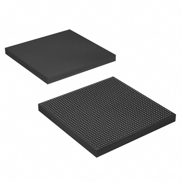
Virtex®-II Pro Field Programmable Gate Array (FPGA) IC 996 6045696 74448 1704-BBGA, FCBGA |
|---|---|
| Quantity | 1,180 Available (as of June 15, 2026) |

| Product Category | Field Programmable Gate Array (FPGA) |
|---|---|
| Manufacturer | AMD |
| Manufacturing Status | Obsolete |
| Manufacturer Standard Lead Time | Contact Us |
| Datasheet |
Specifications & Environmental
| Device Package | 1704-FCBGA (42.5x42.5) | Grade | Commercial | Operating Temperature | 0°C – 85°C | ||
|---|---|---|---|---|---|---|---|
| Package / Case | 1704-BBGA, FCBGA | Number of I/O | 996 | Voltage | 1.425 V - 1.575 V | ||
| Mounting Method | Surface Mount | RoHS Compliance | ROHS3 Compliant | REACH Compliance | REACH Unaffected | ||
| Moisture Sensitivity Level | 4 (72 Hours) | Number of LABs/CLBs | 8272 | Number of Logic Elements/Cells | 74448 | ||
| Number of Gates | N/A | ECCN | 3A001A7A | HTS Code | 8542.39.0001 | ||
| Qualification | N/A | Total RAM Bits | 6045696 |
Overview of XC2VP70-5FFG1704C – Virtex®-II Pro FPGA, 1704‑FCBGA, 74,448 logic elements
The XC2VP70-5FFG1704C is a Virtex®-II Pro field-programmable gate array (FPGA) in a 1704-ball FCBGA package. It integrates a large programmable fabric with on-chip embedded processor block support and high-speed serial/transceiver capabilities, targeting advanced embedded, communications and processing applications that require substantial logic, memory and I/O capacity.
With 74,448 logic elements, approximately 6.05 Mbits of embedded memory and up to 996 I/O pins in a 42.5 × 42.5 mm FCBGA, this device is suited for designs that need high channel density, extensive on-chip resources and on-board integration. Operating supply ranges and commercial temperature grading are provided for system-level planning.
Key Features
- Large programmable fabric — 74,448 logic elements provide extensive logic capacity for complex custom hardware and system acceleration.
- Embedded memory — Approximately 6.05 Mbits of on-chip RAM (total RAM bits: 6,045,696) for buffering, state storage and local data processing.
- High I/O density — Up to 996 user I/O pins support dense board-level interfacing and multi-channel connectivity.
- RocketIO transceiver support — Family-level support for RocketIO/RocketIO X multi-gigabit transceivers, including telecom/datacom modes and programmable signal conditioning features described in the device family documentation.
- Embedded processor block support — Family documentation describes up to two IBM PowerPC RISC processor blocks for embedded-control and system management integration.
- Dedicated DSP and memory primitives — On-chip 18-bit × 18-bit multiplier blocks and SelectRAM™ block RAM resources for DSP and high-throughput data operations.
- Clocking and timing resources — Integrated clock management circuitry and global clock resources to support complex, synchronous designs.
- Power and supply — Device core supply range: 1.425 V to 1.575 V for system power budgeting and regulator selection.
- Package and mounting — 1704-ball FCBGA (42.5 × 42.5 mm) surface-mount package for compact, high-density board designs.
- Commercial temperature grade — Operating range: 0 °C to 85 °C for commercial-temperature deployments.
- RoHS compliant — Conforms to RoHS environmental requirements for lead-free assembly processes.
Typical Applications
- Telecom & Datacom — Multi-gigabit transceiver features and configurable I/O make the device suitable for high-speed serial links, protocol bridging and packet processing.
- Embedded Processing — On-chip processor block support enables system control, protocol offload and embedded software acceleration.
- Signal Processing & Acceleration — Abundant logic, dedicated multiplier blocks and block RAM allow implementation of DSP pipelines, filters and custom accelerators.
- High-Density I/O Systems — Nearly 1,000 I/O pins in a compact FCBGA package support multi-interface aggregation and large sensor or actuator arrays.
Unique Advantages
- Highly integrated resources: Combines a large logic fabric, significant on-chip memory and DSP primitives to reduce external components and simplify board-level design.
- High connectivity: Up to 996 I/O pins provide the flexibility to consolidate multiple interfaces and channels on a single device.
- Embedded processing capability: Family-level PowerPC processor block support enables tighter hardware–software integration for control and protocol tasks.
- Support for high-speed serial interfaces: RocketIO transceiver features described in the family documentation support telecom/datacom signaling modes and programmable transceiver parameters.
- Package density: 1704-FCBGA (42.5 × 42.5 mm) offers a high-pin-count surface-mount solution for compact, high-density boards.
- Clear electrical envelope: Defined core supply range (1.425–1.575 V) and commercial temperature rating (0–85 °C) aid in predictable system integration and power planning.
Why Choose XC2VP70-5FFG1704C?
The XC2VP70-5FFG1704C provides a balanced combination of large logic capacity, substantial embedded memory and high I/O density in a single FCBGA package. It is well suited to designs that demand on-chip processing, extensive interfacing and support for multi-gigabit serial links as described in the Virtex®-II Pro family documentation.
Choose this device for system designs where integration, configurable hardware acceleration and dense connectivity reduce component count and streamline board layout, while meeting commercial temperature and voltage requirements.
Request a quote or submit a purchase inquiry to receive pricing and availability information for the XC2VP70-5FFG1704C.


Date Founded: 1969
Headquarters: Santa Clara, California, USA
Employees: 25,000+
Revenue: $22.68 Billion
Certifications and Memberships: ISO9001:2015, RoHS, REACH


