
XC3SD1800A-5FGG676C
| Part Description |
Spartan®-3A DSP Field Programmable Gate Array (FPGA) IC 519 1548288 37440 676-BGA |
|---|---|
| Quantity | 963 Available (as of June 17, 2026) |

| Product Category | Field Programmable Gate Array (FPGA) |
|---|---|
| Manufacturer | AMD |
| Manufacturing Status | Last Time Buy |
| Manufacturer Standard Lead Time | 12 Weeks |
| Datasheet |
Specifications & Environmental
| Device Package | 676-FBGA (27x27) | Grade | Commercial | Operating Temperature | 0°C – 85°C | ||
|---|---|---|---|---|---|---|---|
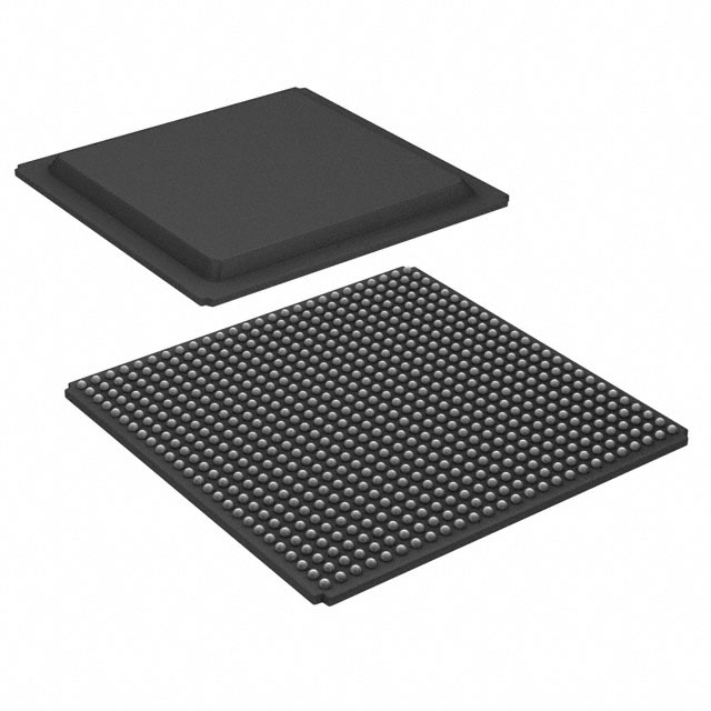
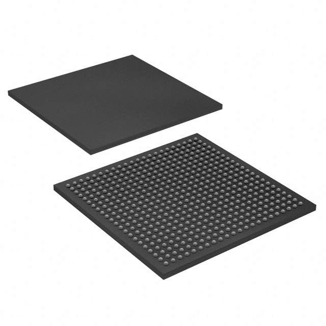
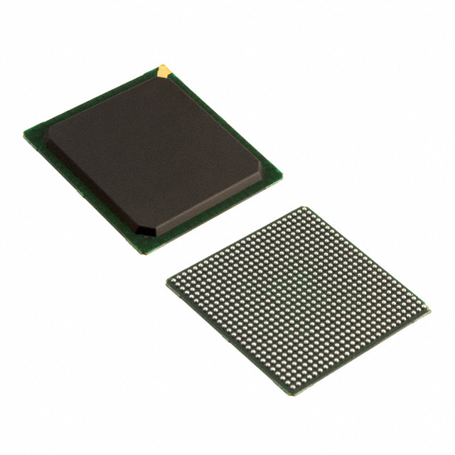
| Package / Case | 676-BGA | Number of I/O | 519 | Voltage | 1.14 V - 1.26 V | ||
| Mounting Method | Surface Mount | RoHS Compliance | ROHS3 Compliant | REACH Compliance | REACH Unaffected | ||
| Moisture Sensitivity Level | 3 (168 Hours) | Number of LABs/CLBs | 4160 | Number of Logic Elements/Cells | 37440 | ||
| Number of Gates | 1800000 | ECCN | 3A001A7A | HTS Code | 8542.39.0001 | ||
| Qualification | N/A | Total RAM Bits | 1548288 |
Overview of XC3SD1800A-5FGG676C – Spartan®-3A DSP Field Programmable Gate Array (FPGA) IC 519 1548288 37440 676-BGA
The XC3SD1800A-5FGG676C is a Spartan®-3A DSP field programmable gate array provided by AMD, combining DSP-oriented FPGA architecture with substantial logic and I/O resources. It targets designs that require dense logic capacity, embedded memory, and a high I/O count in a compact surface-mount package.
This commercial-grade, RoHS-compliant device offers 37,440 logic elements, approximately 1.55 Mbits of on-chip RAM, and 519 I/Os, all delivered in a 676-BGA (676-FBGA 27×27) package with a core voltage range of 1.14–1.26 V and an operating temperature range of 0 °C to 85 °C.
Key Features
- Logic Capacity 37,440 logic elements and 4,160 CLBs provide significant programmable logic resources for complex digital designs.
- Embedded Memory Approximately 1.55 Mbits of on-chip RAM supports buffering, FIFOs, and data-centric DSP functions without relying solely on external memory.
- DSP-Oriented Architecture Spartan®-3A DSP family designation indicates architecture optimized for digital signal processing tasks and algorithm acceleration.
- I/O Density 519 I/O pins enable broad peripheral connectivity and support for multi-channel front-end interfaces or parallel buses.
- Gate Count Approximately 1,800,000 gates for high-density logic implementations and integration of multiple subsystems on a single device.
- Package and Mounting 676-BGA (supplier package: 676-FBGA 27×27) surface-mount package provides a compact footprint for space-constrained PCBs.
- Power and Thermal Core supply range of 1.14–1.26 V and commercial operating temperature range of 0 °C to 85 °C align with typical board-level power and environmental constraints.
- Compliance RoHS compliant for lead-free assembly and regulatory alignment in commercial products.
Typical Applications
- Digital Signal Processing DSP-optimized FPGA resources and on-chip RAM enable acceleration of filters, transforms, and real-time signal algorithms.
- High-Density Logic Integration Large logic element and gate counts allow consolidation of multiple control and processing functions onto a single device to reduce system BOM.
- I/O-Intensive Systems With 519 I/Os, the device is suited for applications requiring numerous parallel interfaces, sensor arrays, or multi-channel data capture.
- Embedded Platform Development The combination of logic, RAM, and I/O density supports prototyping and deployment of custom embedded processing solutions.
Unique Advantages
- High Integration Density: 37,440 logic elements and ~1.8 million gates let designers implement complex functions and reduce external components.
- On-Chip Memory for Real-Time Tasks: Approximately 1.55 Mbits of embedded RAM provides on-chip storage for buffering and low-latency data paths.
- Extensive I/O Count: 519 I/Os enable flexible system interfacing without immediate need for large external I/O expanders.
- Compact, Surface-Mount Package: 676-BGA (676-FBGA 27×27) delivers a high-pin-count solution in a compact form factor for board-level space savings.
- Commercial-Grade Reliability: Rated for 0 °C to 85 °C operation and RoHS compliant for broad commercial product deployment.
- Defined Core Supply Range: Core voltage support of 1.14–1.26 V provides clear power design parameters for system integration.
Why Choose XC3SD1800A-5FGG676C?
The XC3SD1800A-5FGG676C positions itself as a high-capacity, DSP-oriented FPGA that balances logic density, embedded memory, and extensive I/O in a compact 676-BGA package. Its specification set—37,440 logic elements, approximately 1.55 Mbits of on-chip RAM, 519 I/Os, and ~1.8M gates—makes it well suited for designers consolidating processing, control, and I/O functions on a single programmable device.
Engineers and procurement teams seeking a RoHS-compliant, commercial-grade FPGA with clearly defined power and temperature parameters can leverage this device for scalable embedded and DSP-focused designs where on-chip resources and I/O density are critical.
Request a quote or submit an inquiry to receive pricing and availability information for the XC3SD1800A-5FGG676C.


Date Founded: 1969
Headquarters: Santa Clara, California, USA
Employees: 25,000+
Revenue: $22.68 Billion
Certifications and Memberships: ISO9001:2015, RoHS, REACH


