
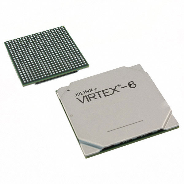
XC6VLX130T-L1FFG1156C
| Part Description |
Virtex®-6 LXT Field Programmable Gate Array (FPGA) IC 600 9732096 128000 1156-BBGA, FCBGA |
|---|---|
| Quantity | 1,688 Available (as of June 15, 2026) |

| Product Category | Field Programmable Gate Array (FPGA) |
|---|---|
| Manufacturer | AMD |
| Manufacturing Status | Active |
| Manufacturer Standard Lead Time | 12 Weeks |
| Datasheet |
Specifications & Environmental
| Device Package | 1156-FCBGA (35x35) | Grade | Commercial | Operating Temperature | 0°C – 85°C | ||
|---|---|---|---|---|---|---|---|
| Package / Case | 1156-BBGA, FCBGA | Number of I/O | 600 | Voltage | 870 mV - 930 mV | ||
| Mounting Method | Surface Mount | RoHS Compliance | ROHS3 Compliant | REACH Compliance | REACH Unaffected | ||
| Moisture Sensitivity Level | 4 (72 Hours) | Number of LABs/CLBs | 10000 | Number of Logic Elements/Cells | 128000 | ||
| Number of Gates | N/A | ECCN | 3A991D | HTS Code | 8542.39.0001 | ||
| Qualification | N/A | Total RAM Bits | 9732096 |
Overview of XC6VLX130T-L1FFG1156C – Virtex®-6 LXT FPGA, 128000 logic elements, 1156-FCBGA
The XC6VLX130T-L1FFG1156C is a Virtex®-6 LXT field programmable gate array (FPGA) IC designed for applications that require high logic density and substantial on-chip memory. It combines a large number of logic elements with extensive embedded RAM and a high I/O count in a compact 1156-FCBGA package.
Targeted at commercial-grade systems, this device provides designers with a configurable hardware platform that supports complex digital designs within a 0 °C to 85 °C operating range and a supply voltage range of 870 mV to 930 mV.
Key Features
- Logic Capacity Provides 128000 logic elements and 10000 CLBs to support complex, high-density digital designs.
- Embedded Memory Includes approximately 9.73 Mbits of on-chip RAM for buffering, lookup tables, and intermediate data storage.
- I/O Resources Offers 600 I/O pins to support wide external connectivity and parallel interfaces.
- Power Operates within a supply voltage range of 870 mV to 930 mV to match system power requirements.
- Package & Mounting Supplied in a 1156-FCBGA (35×35) 1156-BBGA surface-mount package for high-density PCB integration.
- Operating Range & Grade Commercial-grade device rated for 0 °C to 85 °C operation.
- Environmental Compliance RoHS compliant for restricted-substance requirements.
Typical Applications
- High-density digital systems Used where large logic resources (128000 logic elements) are required to implement complex custom logic and control functions.
- Signal processing and buffering Applicable to designs that need substantial on-chip memory—approximately 9.73 Mbits—for data buffering and intermediate storage.
- Connectivity and interface aggregation Suitable for systems requiring a high number of I/O lines (600) to manage multiple parallel or serial interfaces.
- Prototyping and platform development Provides a commercially graded FPGA platform for validating and iterating digital designs within standard temperature and power envelopes.
Unique Advantages
- High logic density: 128000 logic elements enable implementation of large-scale, complex logic functions without external glue logic.
- Significant on-chip memory: Approximately 9.73 Mbits of embedded RAM reduces reliance on external memory and improves data throughput for internal processing.
- Extensive I/O: 600 I/O pins provide flexibility for connecting multiple peripherals, sensors, or high-bandwidth interfaces.
- Compact FCBGA packaging: 1156-FCBGA (35×35) package balances high pin count with a small PCB footprint for space-constrained designs.
- Commercial-grade operating range: Rated 0 °C to 85 °C to match typical commercial applications and system environments.
- Regulatory readiness: RoHS compliance supports environmental and manufacturing requirements.
Why Choose XC6VLX130T-L1FFG1156C?
The XC6VLX130T-L1FFG1156C from AMD combines substantial logic capacity, large embedded RAM, and a high I/O count in a compact FCBGA package, making it well suited for commercial systems that demand dense programmable logic and on-chip memory. Its defined supply voltage range and commercial operating temperature make it a pragmatic choice for mainstream embedded, communications, and digital signal processing designs.
This FPGA is appropriate for designers and teams seeking a scalable, high-capacity programmable fabric that integrates many system functions on-chip, helping reduce board-level complexity and component count while supporting iterative hardware development.
Request a quote or submit an inquiry today to evaluate the XC6VLX130T-L1FFG1156C for your next design project.


Date Founded: 1969
Headquarters: Santa Clara, California, USA
Employees: 25,000+
Revenue: $22.68 Billion
Certifications and Memberships: ISO9001:2015, RoHS, REACH


