
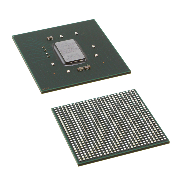
XC7K325T-1FFG676C
| Part Description |
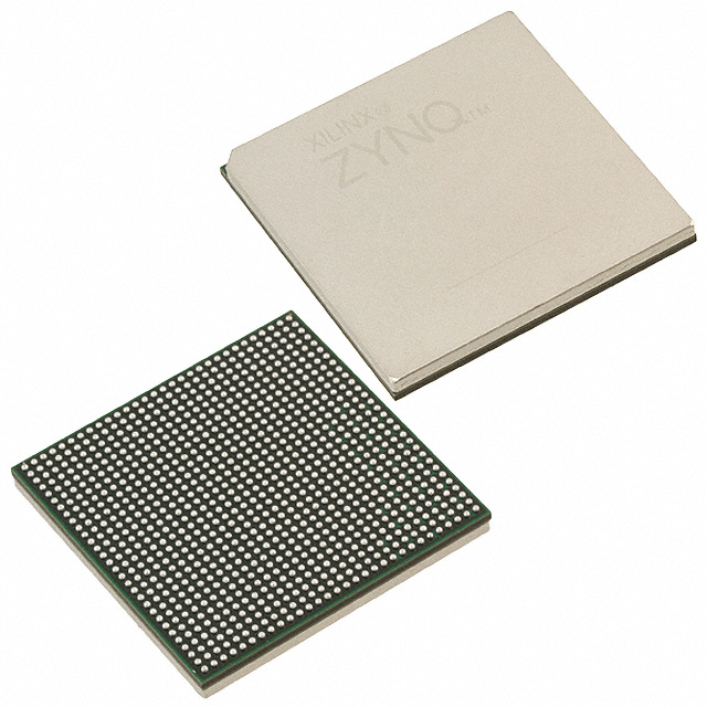
Kintex®-7 Field Programmable Gate Array (FPGA) IC 400 16404480 326080 676-BBGA, FCBGA |
|---|---|
| Quantity | 1,685 Available (as of June 15, 2026) |

| Product Category | Field Programmable Gate Array (FPGA) |
|---|---|
| Manufacturer | AMD |
| Manufacturing Status | Active |
| Manufacturer Standard Lead Time | 16 Weeks |
| Datasheet |
Specifications & Environmental
| Device Package | 676-FCBGA (27x27) | Grade | Commercial | Operating Temperature | 0°C – 85°C | ||
|---|---|---|---|---|---|---|---|
| Package / Case | 676-BBGA, FCBGA | Number of I/O | 400 | Voltage | 970 mV - 1.03 V | ||
| Mounting Method | Surface Mount | RoHS Compliance | ROHS3 Compliant | REACH Compliance | REACH Unaffected | ||
| Moisture Sensitivity Level | 4 (72 Hours) | Number of LABs/CLBs | 25475 | Number of Logic Elements/Cells | 326080 | ||
| Number of Gates | N/A | ECCN | 3A991D | HTS Code | 8542.39.0001 | ||
| Qualification | N/A | Total RAM Bits | 16404480 |
Overview of XC7K325T-1FFG676C – Kintex®-7 Field Programmable Gate Array (FPGA) 676-FCBGA
The XC7K325T-1FFG676C is a Kintex®-7 Field Programmable Gate Array (FPGA) in a high-pin-count 676-FCBGA package. It delivers a combination of large logic capacity, substantial on-chip memory, and a broad I/O count in a commercial-grade, surface-mount device.
Key device attributes include 326,080 logic elements, approximately 16.4 Mbits of embedded memory, 400 I/O pins, a supply voltage range of 970 mV to 1.03 V, and an operating temperature range of 0 °C to 85 °C.
Key Features
- Core logic capacity 326,080 logic elements to support complex programmable logic implementations.
- Embedded memory Approximately 16.4 Mbits of on-chip RAM for data buffering, state storage, and local memory needs.
- High I/O count 400 available I/O pins to accommodate wide parallel interfaces and multiple external peripherals.
- Package and mounting 676-FCBGA (27×27) package; package case listed as 676-BBGA, FCBGA, designed for surface-mount assembly.
- Power supply Core supply range from 970 mV to 1.03 V for the device core domain.
- Operating range and grade Commercial grade device with an operating temperature range of 0 °C to 85 °C.
- Environmental compliance RoHS-compliant to meet lead-free and environmental requirements.
Unique Advantages
- High logic density: 326,080 logic elements provide capacity for sizeable FPGA designs without changing package family.
- Significant on-chip RAM: Approximately 16.4 Mbits of embedded memory reduces the need for external RAM in many designs.
- Extensive I/O connectivity: 400 I/O pins enable flexible interfacing to a variety of external devices and parallel buses.
- Compact, high-pin-count package: 676-FCBGA (27×27) delivers many signals in a compact footprint suitable for surface-mount assembly.
- Clear supply and thermal boundaries: Defined core voltage range (970 mV–1.03 V) and commercial operating temperature (0 °C–85 °C) simplify design validation for commercial applications.
- RoHS compliance: Environmentally compliant manufacturing and assembly compatibility.
Why Choose XC7K325T-1FFG676C?
The XC7K325T-1FFG676C is positioned for designers who require a commercial-grade FPGA with large logic resources, substantial embedded memory, and a high I/O count in a 676-ball FCBGA package. Its specified core voltage range and 0 °C to 85 °C operating window make it suitable for a wide range of commercial embedded systems.
Selecting this Kintex®-7 device supports designs where on-chip resources reduce external component count and where a high number of I/Os and logic elements are essential for system integration and scalability.
Request a quote or submit an inquiry to obtain pricing and availability for the XC7K325T-1FFG676C.


Date Founded: 1969
Headquarters: Santa Clara, California, USA
Employees: 25,000+
Revenue: $22.68 Billion
Certifications and Memberships: ISO9001:2015, RoHS, REACH


