
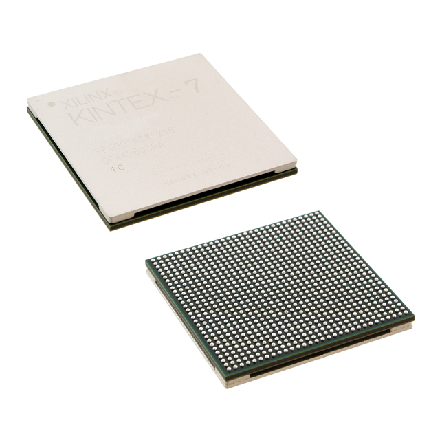
XC7K325T-2FBG900C
| Part Description |
Kintex®-7 Field Programmable Gate Array (FPGA) IC 500 16404480 326080 900-BBGA, FCBGA |
|---|---|
| Quantity | 201 Available (as of June 15, 2026) |

| Product Category | Field Programmable Gate Array (FPGA) |
|---|---|
| Manufacturer | AMD |
| Manufacturing Status | Active |
| Manufacturer Standard Lead Time | 16 Weeks |
| Datasheet |
Specifications & Environmental
| Device Package | 900-FCBGA (31x31) | Grade | Commercial | Operating Temperature | 0°C – 85°C | ||
|---|---|---|---|---|---|---|---|
| Package / Case | 900-BBGA, FCBGA | Number of I/O | 500 | Voltage | 970 mV - 1.03 V | ||
| Mounting Method | Surface Mount | RoHS Compliance | ROHS3 Compliant | REACH Compliance | REACH Unaffected | ||
| Moisture Sensitivity Level | 4 (72 Hours) | Number of LABs/CLBs | 25475 | Number of Logic Elements/Cells | 326080 | ||
| Number of Gates | N/A | ECCN | 3A991D | HTS Code | 8542.39.0001 | ||
| Qualification | N/A | Total RAM Bits | 16404480 |
Overview of XC7K325T-2FBG900C – Kintex®-7 Field Programmable Gate Array (FPGA) IC 500 16404480 326080 900-BBGA, FCBGA
The XC7K325T-2FBG900C is a commercial-grade Kintex®-7 FPGA manufactured by AMD. It delivers a substantial programmable fabric with 326,080 logic elements and approximately 16.4 Mbits of embedded memory, making it suitable for complex digital designs that require high logic density and on-chip storage. Typical use cases include high-performance data-path processing, communications protocol implementation, imaging and vision processing, and advanced prototyping where significant I/O and logic resources are required.
Key Features
- Logic Capacity 326,080 logic elements provide a large programmable fabric for implementing complex custom logic and parallel processing architectures.
- Embedded Memory Approximately 16.4 Mbits of on-chip RAM to support buffering, lookup tables, and intermediate data storage within the FPGA design.
- I/O Density 500 general-purpose I/O pins allow broad interfacing with external devices, high-speed buses, and multi-channel systems.
- Power Supply Core voltage range specified at 0.97 V to 1.03 V for device operation; power sequencing and supply design should follow vendor guidance.
- Package & Mounting 900-ball FCBGA package (900-BBGA, supplier device package: 900-FCBGA 31×31) in a surface-mount form factor for board-level integration.
- Operating Conditions Commercial operating temperature range from 0 °C to 85 °C and RoHS-compliant construction.
Typical Applications
- High-performance signal processing Implement parallel filtering, transforms, and custom datapath logic using the large logic and memory resources.
- Communications and networking Support protocol offload, packet processing, and custom interface logic leveraging 500 I/Os for multi-channel connectivity.
- Imaging and vision systems Accelerate image pipelines and real-time preprocessing with on-chip memory and extensive programmable logic.
- Test, measurement, and instrumentation Create flexible, reconfigurable front-end processing and control logic for lab and production test equipment.
Unique Advantages
- High programmable capacity: 326,080 logic elements enable implementation of large, complex designs without immediate need for external logic.
- Substantial on-chip RAM: Approximately 16.4 Mbits of embedded memory reduces dependency on external SRAM/DRAM for intermediate data storage.
- Generous I/O count: 500 I/Os provide flexibility for multi-channel interfaces, sensor arrays, and high-pin-count connector systems.
- Compact board footprint: 900-ball FCBGA package offers a dense, surface-mount solution for high-resource FPGA integration on space-constrained PCBs.
- Commercial-grade availability: Designed for commercial applications with a 0 °C to 85 °C operating range and RoHS compliance for global manufacturing requirements.
Why Choose XC7K325T-2FBG900C?
The XC7K325T-2FBG900C positions itself as a high-capacity, commercial FPGA option for designs that require substantial programmable logic, embedded memory, and a large number of I/Os in a compact FCBGA package. Its combination of 326,080 logic elements and approximately 16.4 Mbits of on-chip RAM supports complex data-paths and buffering strategies directly inside the device.
This part is well suited for engineering teams developing advanced communications, signal processing, imaging, and test/measurement systems that benefit from reconfigurable hardware. The RoHS-compliant 900-FCBGA package and defined supply and temperature ranges support predictable integration and long-term design planning.
Request a quote or submit an inquiry to get pricing, availability, and further purchasing information for the XC7K325T-2FBG900C.


Date Founded: 1969
Headquarters: Santa Clara, California, USA
Employees: 25,000+
Revenue: $22.68 Billion
Certifications and Memberships: ISO9001:2015, RoHS, REACH


