
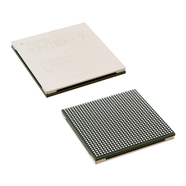
XC7K325T-3FFG900E
| Part Description |
Kintex®-7 Field Programmable Gate Array (FPGA) IC 500 16404480 326080 900-BBGA, FCBGA |
|---|---|
| Quantity | 334 Available (as of June 15, 2026) |

| Product Category | Field Programmable Gate Array (FPGA) |
|---|---|
| Manufacturer | AMD |
| Manufacturing Status | Active |
| Manufacturer Standard Lead Time | 16 Weeks |
| Datasheet |
Specifications & Environmental
| Device Package | 900-FCBGA (31x31) | Grade | Extended | Operating Temperature | 0°C – 100°C | ||
|---|---|---|---|---|---|---|---|
| Package / Case | 900-BBGA, FCBGA | Number of I/O | 500 | Voltage | 970 mV - 1.03 V | ||
| Mounting Method | Surface Mount | RoHS Compliance | ROHS3 Compliant | REACH Compliance | REACH Unaffected | ||
| Moisture Sensitivity Level | 4 (72 Hours) | Number of LABs/CLBs | 25475 | Number of Logic Elements/Cells | 326080 | ||
| Number of Gates | N/A | ECCN | 3A991D | HTS Code | 8542.39.0001 | ||
| Qualification | N/A | Total RAM Bits | 16404480 |
Overview of XC7K325T-3FFG900E – Kintex®-7 FPGA, 900‑FCBGA, 326,080 logic elements
The XC7K325T-3FFG900E is a Kintex®-7 field programmable gate array (FPGA) IC from AMD, delivered in a 900‑ball FCBGA (31 × 31) package. It integrates a high-density logic fabric with extensive on-chip memory and a large I/O complement for complex digital designs.
This device targets designs that require substantial logic capacity, embedded memory and flexible I/O count while operating within a supply range of 0.97 V to 1.03 V and an operating temperature range of 0 °C to 100 °C. It is supplied in a surface-mount package and is RoHS compliant.
Key Features
- Logic Capacity 326,080 logic elements provide significant programmable logic resources for complex state machines, datapaths and custom accelerators.
- Embedded Memory Approximately 16 Mbits of on-chip RAM (16,404,480 bits) to support buffering, frame storage and algorithmic data handling without external memory in many use cases.
- I/O Resources 500 user I/O pins to support wide parallel interfaces, multiple protocol domains and extensive peripheral connectivity.
- Package and Mounting 900‑ball FCBGA package (31 × 31) optimized for high-density routing; surface-mount mounting type suitable for modern PCB assembly.
- Power Core supply voltage range of 0.97 V to 1.03 V to align with system power delivery designs for the Kintex-7 device.
- Operating Conditions Extended grade with an operating temperature range of 0 °C to 100 °C for deployment in temperature-controlled and commercial environments.
- Compliance RoHS compliant, supporting regulatory requirements for lead-free assembly.
Typical Applications
- High-throughput signal processing — Use the 326,080 logic elements and approximately 16 Mbits of embedded memory to implement filters, FFTs and other DSP blocks with large on-chip buffering.
- Data plane acceleration — 500 I/Os allow wide parallel and multi-protocol interfaces for packet processing, accelerator front-ends or custom network logic.
- Image and video processing — Large logic and memory resources support frame buffering, pixel pipelines and real-time processing chains.
- Embedded compute and control — Integrate control logic, interfacing and local data storage in a single FPGA package for compact system designs.
Unique Advantages
- Large programmable fabric: 326,080 logic elements provide headroom for complex algebraic implementations and parallel processing engines.
- Substantial on-chip memory: Approximately 16 Mbits of RAM reduces dependence on external memory for many buffering and caching tasks.
- Generous I/O count: 500 I/Os enable flexible connectivity options for multi-channel interfaces and mixed-signal front-ends.
- Compact, production-ready package: 900‑ball FCBGA (31 × 31) supports high-density PCB layouts and automated surface-mount assembly.
- Predictable power window: Specified core supply range of 0.97 V to 1.03 V simplifies power-supply design and margin planning.
- Extended-grade operating range: Rated for 0 °C to 100 °C to align with a wide set of commercial and controlled-environment deployments.
Why Choose XC7K325T-3FFG900E?
The XC7K325T-3FFG900E combines a high-density Kintex-7 FPGA fabric with approximately 16 Mbits of embedded RAM and 500 I/Os in a 900‑ball FCBGA package, making it well-suited for designs that demand significant on-chip logic and memory integration. Its defined core voltage range and extended operating temperature provide clear parameters for power and thermal planning.
This device is appropriate for engineering teams building complex signal processing, data acceleration or embedded compute solutions that benefit from large programmable resources and a robust I/O complement, while maintaining RoHS compliance for modern assembly workflows.
Request a quote or submit an inquiry for the XC7K325T-3FFG900E to evaluate pricing and availability for your project requirements.


Date Founded: 1969
Headquarters: Santa Clara, California, USA
Employees: 25,000+
Revenue: $22.68 Billion
Certifications and Memberships: ISO9001:2015, RoHS, REACH


