
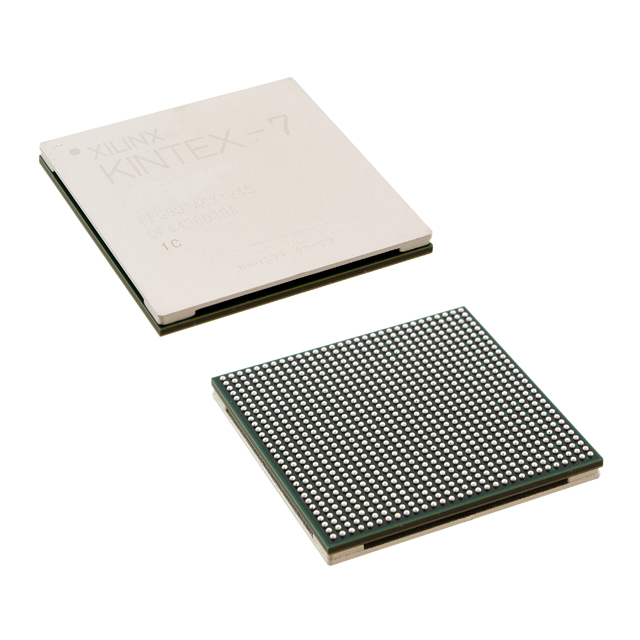
XC7K325T-L2FBG676E
| Part Description |
Kintex®-7 Field Programmable Gate Array (FPGA) IC 400 16404480 326080 676-BBGA, FCBGA |
|---|---|
| Quantity | 1,433 Available (as of June 15, 2026) |

| Product Category | Field Programmable Gate Array (FPGA) |
|---|---|
| Manufacturer | AMD |
| Manufacturing Status | Active |
| Manufacturer Standard Lead Time | 16 Weeks |
| Datasheet |
Specifications & Environmental
| Device Package | 676-FCBGA (27x27) | Grade | Extended | Operating Temperature | 0°C – 100°C | ||
|---|---|---|---|---|---|---|---|
| Package / Case | 676-BBGA, FCBGA | Number of I/O | 400 | Voltage | 970 mV - 1.03 V | ||
| Mounting Method | Surface Mount | RoHS Compliance | ROHS3 Compliant | REACH Compliance | REACH Unaffected | ||
| Moisture Sensitivity Level | 4 (72 Hours) | Number of LABs/CLBs | 25475 | Number of Logic Elements/Cells | 326080 | ||
| Number of Gates | N/A | ECCN | 3A991D | HTS Code | 8542.39.0001 | ||
| Qualification | N/A | Total RAM Bits | 16404480 |
Overview of XC7K325T-L2FBG676E – Kintex®-7 Field Programmable Gate Array (FPGA)
The XC7K325T-L2FBG676E is a Kintex®-7 family field programmable gate array (FPGA) offered in a 676-ball fine-pitch BGA package. It provides a large on-chip resource set including 326,080 logic elements, approximately 16.4 Mbits of embedded memory, and 400 user I/Os for designs that require high logic and I/O density.
This device is supplied for surface-mount PCB assembly in a 676-FCBGA (27×27) package, operates with a core voltage range of 970 mV to 1.03 V, and is specified for operation from 0 °C to 100 °C with an Extended grade and RoHS compliance.
Key Features
- Core Logic 326,080 logic elements (cells) provide substantial capacity for complex programmable logic implementations.
- Embedded Memory Approximately 16.4 Mbits of on-chip RAM for buffering, state storage, and local data processing without external memory.
- I/O Count 400 user I/Os to support high-density interfacing to peripherals, sensors, and other system components.
- Package and Mounting 676-BBGA / 676-FCBGA (27×27) in a surface-mount form factor to fit compact, high-density board layouts.
- Power Supply Core voltage specified between 970 mV and 1.03 V to match system power delivery design requirements.
- Operating Range & Grade Extended grade device rated for 0 °C to 100 °C operation, suitable for applications within that temperature window.
- Regulatory RoHS compliant, meeting common requirements for lead-free assembly.
Typical Applications
- Data Processing and Acceleration Large logic capacity and embedded memory enable implementation of application-specific data paths and buffering on-chip.
- High-Density I/O Systems 400 user I/Os support complex I/O connectivity for systems requiring numerous interfaces or parallel buses.
- Custom Logic Integration Consolidate multiple discrete functions into a single FPGA using substantial logic and memory resources to simplify board-level design.
Unique Advantages
- Substantial Logic Capacity: 326,080 logic elements allow integration of wide-ranging programmable functions within one device.
- On-Chip Memory Resources: Approximately 16.4 Mbits of embedded RAM reduce dependence on external memory for many buffering and scratchpad needs.
- High I/O Count: 400 user I/Os support extensive peripheral interfacing and flexible system partitioning.
- Compact Surface-Mount Package: 676-FCBGA (27×27) gives a balance of high integration and a board footprint suitable for dense designs.
- Controlled Power Envelope: Defined core voltage range (970 mV–1.03 V) assists in precise power-supply planning for system integration.
- Extended Temperature Grade: Rated for 0 °C to 100 °C operation to meet a broad set of commercial and extended-temperature applications.
Why Choose XC7K325T-L2FBG676E?
The XC7K325T-L2FBG676E combines a large logic fabric, significant embedded memory, and a high I/O count in a compact 676-ball BGA package, making it well suited to designs that need dense programmable logic and extensive interfacing in a single device. Its specified core voltage range and 0 °C to 100 °C operating window provide clear electrical and thermal design parameters for system integration.
For development teams and procurement seeking a Kintex®-7 FPGA with defined resources—326,080 logic elements, approximately 16.4 Mbits of on-chip RAM, 400 I/Os, and RoHS compliance—this part delivers a verifiable set of capabilities for high-density programmable designs.
Request a quote or submit a purchase inquiry to receive pricing and availability for the XC7K325T-L2FBG676E.


Date Founded: 1969
Headquarters: Santa Clara, California, USA
Employees: 25,000+
Revenue: $22.68 Billion
Certifications and Memberships: ISO9001:2015, RoHS, REACH


