
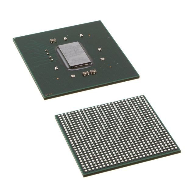
XC7K355T-L2FFG901I
| Part Description |
Kintex®-7 Field Programmable Gate Array (FPGA) IC 300 26357760 356160 900-BBGA, FCBGA |
|---|---|
| Quantity | 1,340 Available (as of June 15, 2026) |

| Product Category | Field Programmable Gate Array (FPGA) |
|---|---|
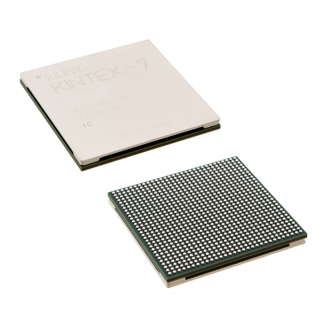
| Manufacturer | AMD |
| Manufacturing Status | Active |
| Manufacturer Standard Lead Time | 16 Weeks |
| Datasheet |
Specifications & Environmental
| Device Package | 901-FCBGA (31x31) | Grade | Industrial | Operating Temperature | -40°C – 100°C | ||
|---|---|---|---|---|---|---|---|
| Package / Case | 900-BBGA, FCBGA | Number of I/O | 300 | Voltage | 970 mV - 1.03 V | ||
| Mounting Method | Surface Mount | RoHS Compliance | ROHS3 Compliant | REACH Compliance | REACH Unaffected | ||
| Moisture Sensitivity Level | 4 (72 Hours) | Number of LABs/CLBs | 27825 | Number of Logic Elements/Cells | 356160 | ||
| Number of Gates | N/A | ECCN | 3A991D | HTS Code | 8542.39.0001 | ||
| Qualification | N/A | Total RAM Bits | 26357760 |
Overview of XC7K355T-L2FFG901I – Kintex®-7 FPGA, 300 I/O, ~26.36 Mbits RAM, 356,160 Logic Elements
The XC7K355T-L2FFG901I is a Kintex®-7 Field Programmable Gate Array (FPGA) from AMD designed for applications requiring substantial on-chip logic and memory resources. With 356,160 logic elements and approximately 26.36 Mbits of embedded memory, this industrial-grade, surface-mount device delivers integrated capacity for complex custom logic, buffering, and data processing.
Key attributes—300 user I/O, an industrial operating temperature range, and a compact FCBGA package—make the device suitable for designs that need high logic density, significant embedded memory, and robust thermal performance within the specified supply and temperature limits.
Key Features
- Logic Capacity — 356,160 logic elements provide extensive resources for implementing complex algorithms, parallel datapaths, and large-scale state machines.
- Embedded Memory — Approximately 26.36 Mbits of on-chip RAM to support buffering, FIFOs, and local data storage without external memory dependence.
- I/O Resources — 300 user I/O pins to interface with sensors, peripherals, and high-density board-level interconnects.
- Power Supply — Core supply range of 0.97 V to 1.03 V to match system power-rail requirements and enable deterministic power planning.
- Package and Mounting — 900-BBGA FCBGA package; supplier device package listed as 901-FCBGA (31×31). Surface-mount mounting type for compact PCB integration.
- Industrial Temperature Range — Rated for operation from -40 °C to 100 °C to meet extended-environment requirements.
- Regulatory Compliance — RoHS compliant, supporting regulatory and environmental considerations in product design.
Typical Applications
- High-density logic implementations — Use the large logic element count to consolidate multiple functions into a single FPGA for compact, integrated board designs.
- On-chip buffering and data handling — Leverage approximately 26.36 Mbits of embedded RAM for local data storage, DMA buffering, and streaming applications.
- Industrial control and automation — Industrial temperature rating and extensive I/O make the device suitable for control systems, machine interfaces, and real-time processing in industrial environments.
- Prototype and custom IP integration — High logic and memory resources accommodate development and deployment of custom IP cores and complex prototyping tasks.
Unique Advantages
- Large integrated logic pool: 356,160 logic elements reduce the need for multiple discrete devices, simplifying system architecture and lowering BOM complexity.
- Significant on-chip memory: Approximately 26.36 Mbits of embedded RAM enables efficient local data storage and reduced external memory dependency, improving latency and board-level cost.
- Ample I/O flexibility: 300 I/O pins support dense peripheral connections and flexible board routing for mixed-signal and digital interfaces.
- Industrial-grade thermal range: Rated from -40 °C to 100 °C to support deployment in harsher environmental conditions without additional thermal qualification effort.
- Compact surface-mount packaging: FCBGA package (901-FCBGA, 31×31) enables space-efficient PCB designs while maintaining high pin count and signal density.
- Regulatory alignment: RoHS compliance assists in meeting environmental and regulatory requirements for manufactured products.
Why Choose XC7K355T-L2FFG901I?
The XC7K355T-L2FFG901I positions itself as a high-capacity Kintex®-7 FPGA option for designs that demand extensive logic resources and substantial embedded memory within a compact, industrial-grade package. Its combination of 356,160 logic elements, approximately 26.36 Mbits of on-chip RAM, and 300 I/O pins supports consolidation of complex functionality onto a single device, reducing system complexity and board-level components.
This device is well suited to engineering teams building applications that require scalable logic density, robust thermal performance from -40 °C to 100 °C, and deterministic supply requirements (0.97 V to 1.03 V). Its surface-mount FCBGA package and RoHS compliance further support modern manufacturing and environmental requirements.
Request a quote or submit an inquiry to receive pricing and availability for the XC7K355T-L2FFG901I.


Date Founded: 1969
Headquarters: Santa Clara, California, USA
Employees: 25,000+
Revenue: $22.68 Billion
Certifications and Memberships: ISO9001:2015, RoHS, REACH


