
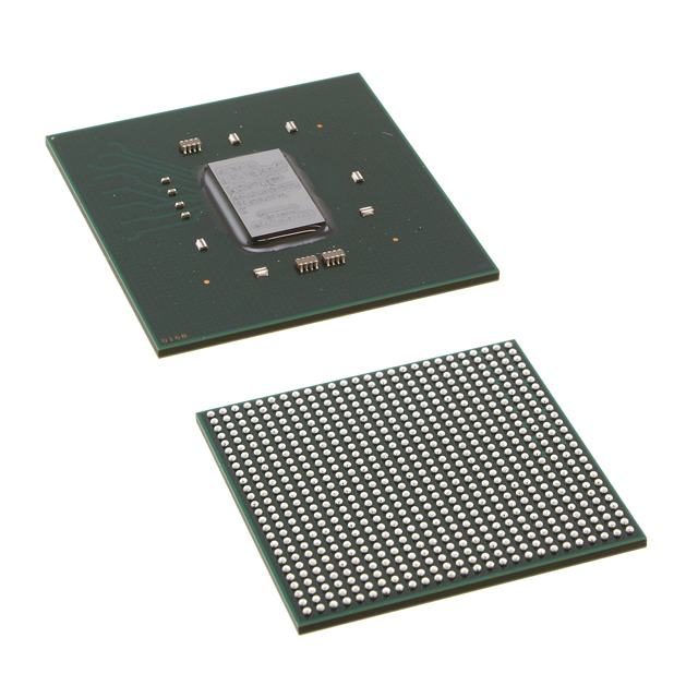
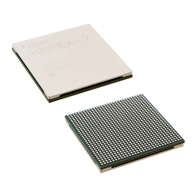
XC7K410T-1FBG676I
| Part Description |
Kintex®-7 Field Programmable Gate Array (FPGA) IC 400 29306880 406720 676-BBGA, FCBGA |
|---|---|
| Quantity | 826 Available (as of October 8, 2026) |
| Product Category | Field Programmable Gate Array (FPGA) |
|---|---|
| Manufacturer | AMD |
| Manufacturing Status | Active |
| Manufacturer Standard Lead Time | 16 Weeks |
| Datasheet |
Specifications & Environmental
| Device Package | 676-FCBGA (27x27) | Grade | Industrial | Operating Temperature | -40°C – 100°C | ||
|---|---|---|---|---|---|---|---|
| Package / Case | 676-BBGA, FCBGA | Number of I/O | 400 | Voltage | 970 mV - 1.03 V | ||
| Mounting Method | Surface Mount | RoHS Compliance | ROHS3 Compliant | REACH Compliance | REACH Unaffected | ||
| Moisture Sensitivity Level | 4 (72 Hours) | Number of LABs/CLBs | 31775 | Number of Logic Elements/Cells | 406720 | ||
| Number of Gates | N/A | ECCN | 3A991D | HTS Code | 8542.39.0001 | ||
| Qualification | N/A | Total RAM Bits | 29306880 |
Overview of XC7K410T-1FBG676I – Kintex®-7 FPGA, 676‑FCBGA, Industrial
The XC7K410T-1FBG676I is a Kintex®-7 field programmable gate array (FPGA) in a 676‑ball FCBGA package designed for industrial applications. It combines high logic density with substantial on‑chip memory and a broad I/O count to support complex, compute‑intensive designs.
Key attributes include approximately 406,720 logic elements, roughly 29.3 Mbits of embedded memory, 400 user I/Os, and an industrial operating range from -40 °C to 100 °C, making it suitable for demanding embedded and industrial systems that require low‑voltage operation around 0.97–1.03 V.
Key Features
- Core Logic Approximately 406,720 logic elements for implementing large, parallelizable logic and custom processing pipelines.
- Embedded Memory Approximately 29.3 Mbits of on‑chip RAM to support data buffering, frame storage, and state machines without external memory in many designs.
- I/O Capacity 400 user I/O pins to interface with sensors, transceivers, ADCs/DACs, and other system peripherals.
- Power Core voltage supply specified from 970 mV to 1.03 V to match low‑voltage system rails and enable optimized power budgeting.
- Package & Mounting 676‑ball FCBGA (27 × 27 mm supplier package) in a surface‑mount form factor for dense PCB integration.
- Temperature & Grade Industrial grade with operating temperature from -40 °C to 100 °C for reliable operation in a wide range of environments.
- Compliance RoHS compliant to meet common environmental and manufacturing requirements.
Typical Applications
- Industrial Control — Implement real‑time control loops, motor control logic, and deterministic I/O aggregation using the FPGA's large logic and I/O resources.
- Data Acquisition & Signal Processing — Use abundant embedded memory and logic density for high‑throughput filtering, buffering, and preprocessing of sensor data.
- Communications Infrastructure — Deploy protocol bridging, packet processing, and custom interface logic where high I/O count and programmable hardware acceleration are required.
- Test & Measurement — Build flexible measurement front ends and pattern generators leveraging on‑chip RAM and sizable logic capacity for timing and control.
Unique Advantages
- High Logic Density: Approximately 406,720 logic elements allow implementation of complex, multi‑functional designs on a single device, reducing the need for external controllers.
- Substantial On‑Chip Memory: Approximately 29.3 Mbits of embedded RAM enable large buffers and state storage, simplifying memory architecture and lowering BOM count.
- Extensive I/O Count: 400 user I/Os provide flexible connectivity options for interfacing with a wide range of peripherals and transceivers.
- Industrial Reliability: Specified for -40 °C to 100 °C operation and offered in a robust surface‑mount FCBGA package suitable for industrial deployments.
- Low‑Voltage Core: Core supply range of 970 mV to 1.03 V supports modern low‑voltage system designs and helps with power optimization strategies.
- Regulatory Compliance: RoHS compliance supports environmentally conscious manufacturing requirements.
Why Choose XC7K410T-1FBG676I?
The XC7K410T-1FBG676I delivers a balance of high logic capacity, significant embedded memory, and a large I/O footprint in a compact 676‑ball FCBGA package, targeting industrial applications that require reliable, programmable hardware. Its operating range and low‑voltage core make it suitable for systems that must operate across extended temperature ranges while maintaining efficient power characteristics.
This device is well suited to engineers developing complex signal processing, control, and I/O‑heavy systems who need a single, scalable FPGA platform to consolidate functions, reduce board complexity, and shorten design cycles.
Request a quote or submit an inquiry to receive pricing and availability for the XC7K410T-1FBG676I.





















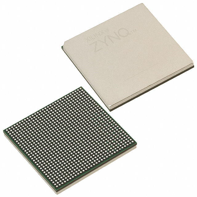


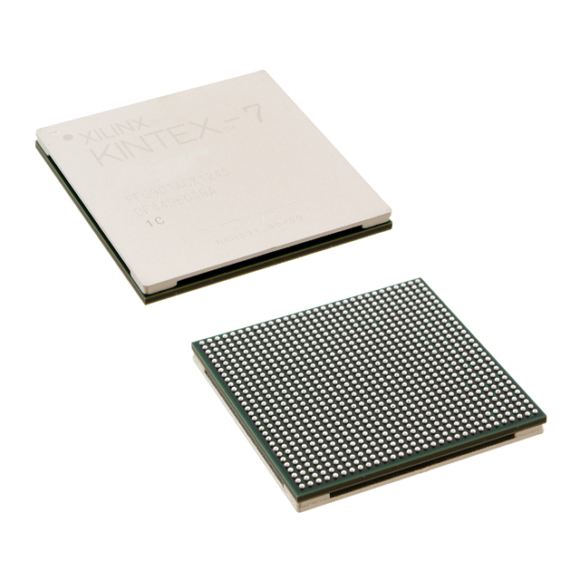
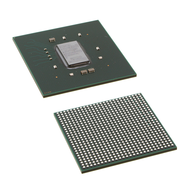


Date Founded: 1969
Headquarters: Santa Clara, California, USA
Employees: 25,000+
Revenue: $22.68 Billion
Certifications and Memberships: ISO9001:2015, RoHS, REACH











