
XC7K410T-2FBG676C
| Part Description |
Kintex®-7 Field Programmable Gate Array (FPGA) IC 400 29306880 406720 676-BBGA, FCBGA |
|---|---|
| Quantity | 1,196 Available (as of June 15, 2026) |
| Product Category | Field Programmable Gate Array (FPGA) |
|---|---|
| Manufacturer | AMD |
| Manufacturing Status | Active |
| Manufacturer Standard Lead Time | 16 Weeks |
| Datasheet |
Specifications & Environmental
| Device Package | 676-FCBGA (27x27) | Grade | Commercial | Operating Temperature | 0°C – 85°C | ||
|---|---|---|---|---|---|---|---|
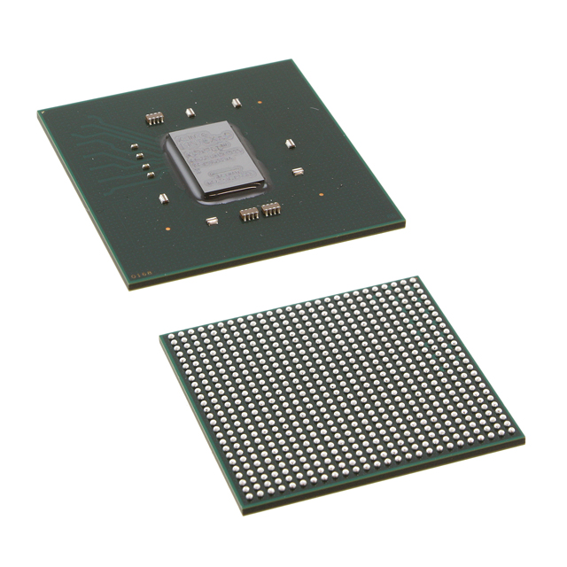
| Package / Case | 676-BBGA, FCBGA | Number of I/O | 400 | Voltage | 970 mV - 1.03 V | ||
| Mounting Method | Surface Mount | RoHS Compliance | ROHS3 Compliant | REACH Compliance | REACH Unaffected | ||
| Moisture Sensitivity Level | 4 (72 Hours) | Number of LABs/CLBs | 31775 | Number of Logic Elements/Cells | 406720 | ||
| Number of Gates | N/A | ECCN | 3A991D | HTS Code | 8542.39.0001 | ||
| Qualification | N/A | Total RAM Bits | 29306880 |
Overview of XC7K410T-2FBG676C – Kintex®-7 FPGA, 406,720 logic cells, 400 I/O, 676-FCBGA
The XC7K410T-2FBG676C is a Kintex®-7 Field Programmable Gate Array (FPGA) IC from AMD, offering a high density of programmable logic and on-chip memory. Key device metrics include 406,720 logic cells, approximately 29.3 Mbits of on-chip RAM, and 400 user I/O pins.
This commercial-grade, surface-mount FCBGA device is specified for a core voltage range of 0.970–1.03 V and an operating temperature range of 0 °C to 85 °C, delivered in a 676-FCBGA (27×27) package suitable for compact, high-pin-count board designs.
Key Features
- Core Logic 406,720 logic cells provide extensive programmable logic resources for complex digital designs.
- On-Chip Memory Approximately 29.3 Mbits of total RAM bits for buffering, state storage, and memory-intensive logic functions.
- I/O Capacity 400 I/O pins support dense external connectivity and interface options on high-channel designs.
- Power Supply Specified core voltage range from 0.970 V to 1.03 V for the device core.
- Package & Mounting 676-FCBGA (27×27) package in a surface-mount format for high I/O density in compact layouts.
- Temperature & Grade Commercial-grade device with an operating temperature range of 0 °C to 85 °C.
- Environmental Compliance RoHS-compliant construction.
Unique Advantages
- High-density programmable fabric: 406,720 logic cells enable large-scale logic integration without immediate external FPGA expansion.
- Substantial embedded memory: Approximately 29.3 Mbits of on-chip RAM reduces dependence on external memory for latency-sensitive buffering and data paths.
- Generous I/O count: 400 user I/Os support multiple parallel interfaces and high-channel systems on a single device.
- Compact, high-pin-count package: 676-FCBGA (27×27) provides a balance of pin density and board-level footprint for space-constrained designs.
- Commercial-grade thermal range: Specified 0 °C to 85 °C operation for standard commercial applications.
- RoHS compliant: Meets common environmental requirements for electronic assemblies.
Why Choose XC7K410T-2FBG676C?
The XC7K410T-2FBG676C delivers a combination of high logic capacity, ample embedded RAM, and extensive I/O in a single Kintex-7 FPGA package from AMD. Its specifications make it suitable for commercial designs that require significant on-chip resources and a compact, surface-mount FCBGA footprint.
For designers seeking a commercially graded, high-density FPGA with defined core voltage and operating-temperature limits, this part offers clear, verifiable device-level attributes that support scalable and integrated digital designs within the Kintex-7 family.
Request a quote or submit an inquiry for XC7K410T-2FBG676C to obtain pricing, availability, and ordering information.


Date Founded: 1969
Headquarters: Santa Clara, California, USA
Employees: 25,000+
Revenue: $22.68 Billion
Certifications and Memberships: ISO9001:2015, RoHS, REACH


