
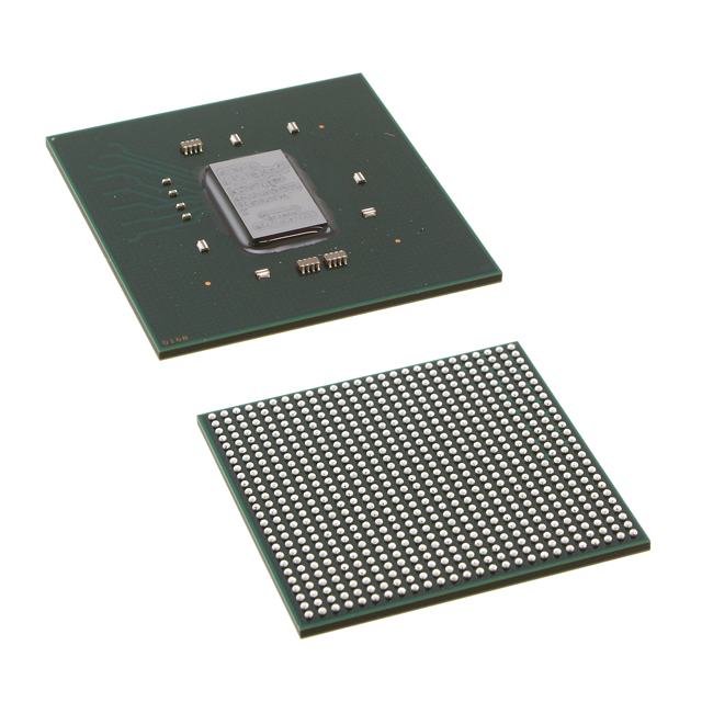
XC7S100-1FGGA676C
| Part Description |
Spartan®-7 Field Programmable Gate Array (FPGA) IC 400 4423680 102400 676-BGA |
|---|---|
| Quantity | 105 Available (as of June 14, 2026) |

| Product Category | Field Programmable Gate Array (FPGA) |
|---|---|
| Manufacturer | AMD |
| Manufacturing Status | Active |
| Manufacturer Standard Lead Time | 16 Weeks |
| Datasheet |
Specifications & Environmental
| Device Package | 676-FPBGA (27x27) | Grade | Commercial | Operating Temperature | 0°C – 85°C | ||
|---|---|---|---|---|---|---|---|
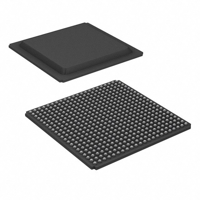
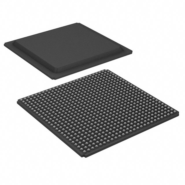
| Package / Case | 676-BGA | Number of I/O | 400 | Voltage | 950 mV - 1.05 V | ||
| Mounting Method | Surface Mount | RoHS Compliance | ROHS3 Compliant | REACH Compliance | REACH Unknown | ||
| Moisture Sensitivity Level | 3 (168 Hours) | Number of LABs/CLBs | 8000 | Number of Logic Elements/Cells | 102400 | ||
| Number of Gates | N/A | ECCN | 5A002A1 | HTS Code | 8542.39.0001 | ||
| Qualification | N/A | Total RAM Bits | 4423680 |
Overview of XC7S100-1FGGA676C – Spartan®-7 FPGA, 400 I/Os, 102,400 logic elements, 676-BGA
The XC7S100-1FGGA676C is a Spartan®-7 Field Programmable Gate Array (FPGA) IC from AMD designed for commercial-grade applications. It combines a substantial logic capacity with on-chip memory and a high pin count in a compact 676-ball BGA package to address mid-range programmable-logic requirements.
Key capabilities include approximately 102,400 logic elements, roughly 4.42 Mbits of embedded RAM, up to 400 I/O pins, and a low-voltage core supply range. The device is supplied in a 676-FPBGA (27×27) surface-mount package and specified for operation from 0 °C to 85 °C.
Key Features
- Core Logic Approximately 102,400 logic elements for implementing combinational and sequential logic functions across a wide range of commercial designs.
- Embedded Memory Approximately 4.42 Mbits of on-chip RAM provides local storage for buffers, FIFOs, and algorithm state without external memory in many designs.
- I/O Density Up to 400 I/O pins enable support for numerous parallel interfaces, sensor arrays, or mixed-signal front-ends requiring many external connections.
- Power Supply Core voltage specified from 0.95 V to 1.05 V to support low-voltage system architectures and predictable power design.
- Package & Mounting Delivered in a 676-FPBGA (27×27) surface-mount package (676-BGA), providing a compact, high-density footprint for space-constrained PCBs.
- Operating Range Commercial operating temperature range of 0 °C to 85 °C suitable for standard commercial applications.
- Regulatory Compliance RoHS compliant to meet common environmental and manufacturing requirements.
Typical Applications
- Commercial embedded systems Use as the programmable logic core for mid-range embedded platforms where sizable logic capacity and on-chip memory reduce external component count.
- I/O-dense interface modules Ideal for modules that require many parallel or mixed I/O connections, leveraging up to 400 I/Os for camera, display, or sensor aggregation.
- Memory-intensive processing On-chip RAM supports local buffering and intermediate storage for algorithms that benefit from fast, embedded memory access.
- Evaluation and prototyping A compact BGA package and commercial-grade specification make the device suitable for development boards and proof-of-concept hardware.
Unique Advantages
- High logic capacity: Approximately 102,400 logic elements let you implement complex logic blocks and parallel functions without immediate partitioning.
- Substantial embedded memory: Around 4.42 Mbits of on-chip RAM reduces reliance on external memory for many buffering and storage needs.
- Large I/O count: Up to 400 I/Os simplifies integration of multiple peripherals and parallel interfaces, minimizing external multiplexing.
- Compact, high-density package: The 676-FPBGA (27×27) surface-mount package balances pin count and PCB area for compact system designs.
- Low-voltage core operation: Core supply range of 0.95 V to 1.05 V supports power-sensitive architectures and predictable power budgeting.
- Commercial-grade suitability: Rated for 0 °C to 85 °C operation and RoHS compliant for standard commercial product deployments.
Why Choose XC7S100-1FGGA676C?
The XC7S100-1FGGA676C positions itself as a capable commercial-grade FPGA for designs that require a balance of logic density, embedded memory, and a high I/O count in a compact BGA footprint. Its combination of approximately 102,400 logic elements, about 4.42 Mbits of on-chip RAM, and up to 400 I/Os addresses a wide range of mid-range programmable logic needs while keeping PCB area and component count under control.
Manufactured by AMD and delivered in a 676-FPBGA surface-mount package with RoHS compliance, this device is intended for engineering teams developing commercial embedded systems, I/O-heavy modules, memory-dependent processing tasks, and prototype platforms that demand predictable electrical and thermal characteristics.
Request a quote or submit an inquiry to receive pricing and availability information for the XC7S100-1FGGA676C.


Date Founded: 1969
Headquarters: Santa Clara, California, USA
Employees: 25,000+
Revenue: $22.68 Billion
Certifications and Memberships: ISO9001:2015, RoHS, REACH


