
XCKU035-1FBVA676C
| Part Description |
Kintex® UltraScale™ Field Programmable Gate Array (FPGA) IC 312 19456000 444343 676-BBGA, FCBGA |
|---|---|
| Quantity | 893 Available (as of June 15, 2026) |
| Product Category | Field Programmable Gate Array (FPGA) |
|---|---|
| Manufacturer | AMD |
| Manufacturing Status | Active |
| Manufacturer Standard Lead Time | 16 Weeks |
| Datasheet |
Specifications & Environmental
| Device Package | 676-FCBGA (27x27) | Grade | Commercial | Operating Temperature | 0°C – 85°C | ||
|---|---|---|---|---|---|---|---|
| Package / Case | 676-BBGA, FCBGA | Number of I/O | 312 | Voltage | 922 mV - 979 mV | ||
| Mounting Method | Surface Mount | RoHS Compliance | ROHS3 Compliant | REACH Compliance | REACH Unaffected | ||
| Moisture Sensitivity Level | 4 (72 Hours) | Number of LABs/CLBs | 25391 | Number of Logic Elements/Cells | 444343 | ||
| Number of Gates | N/A | ECCN | 3A991D | HTS Code | 8542.39.0001 | ||
| Qualification | N/A | Total RAM Bits | 19456000 |
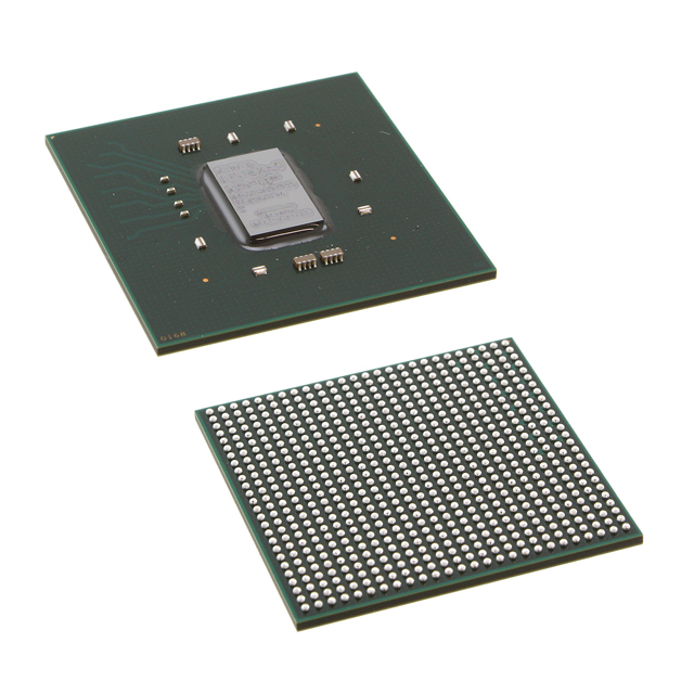
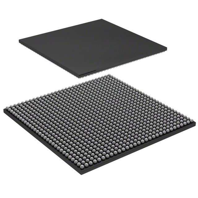
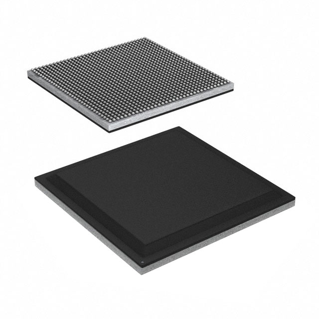
Overview of XCKU035-1FBVA676C – Kintex® UltraScale™ Field Programmable Gate Array, 676-FCBGA
The XCKU035-1FBVA676C is a Kintex® UltraScale™ Field Programmable Gate Array (FPGA) IC by AMD, supplied in a 676-FCBGA (27×27) package for surface-mount applications. It delivers high logic density and on-chip memory capacity for designs that require substantial programmable logic and I/O integration.
Key device attributes include 444,343 logic elements, approximately 19.46 Mbits of embedded memory, and 312 I/O pins. The device operates from 922 mV to 979 mV, is rated for commercial temperature use (0 °C to 85 °C), and is RoHS compliant.
Key Features
- Core Density 444,343 logic elements provide a large programmable fabric for complex digital logic and system integration.
- Embedded Memory Approximately 19.46 Mbits of on-chip RAM to support buffering, lookup tables, and local data storage without external memory.
- I/O Capacity 312 general-purpose I/O pins enable extensive device interfacing and high pin-count connectivity for multi-signal systems.
- Package & Mounting 676-FCBGA (27×27) package in a surface-mount format supports compact board-level integration and high-density PCB layouts.
- Power Specified core voltage range from 922 mV to 979 mV for the device core supply.
- Temperature & Grade Commercial grade operation from 0 °C to 85 °C for standard temperature-range applications.
- Environmental Compliance RoHS compliant to support regulatory and assembly requirements.
Typical Applications
- High-density digital systems Use the device where a large number of logic elements and significant on-chip RAM are required to implement complex state machines, custom datapaths, or large LUT-based functions.
- Multi-channel I/O aggregation Leverage 312 I/O pins to consolidate and route numerous interfaces or signals on a single programmable device.
- Embedded memory-centric designs Employ the approximately 19.46 Mbits of embedded RAM for buffering, packet queuing, or local data stores to reduce external memory dependency.
Unique Advantages
- High logic integration: 444,343 logic elements enable implementation of large, integrated digital functions on a single FPGA, reducing the need for multiple discrete devices.
- Substantial on-chip RAM: Approximately 19.46 Mbits of embedded memory supports significant local storage and buffering, simplifying memory architecture.
- Extensive I/O count: 312 I/O pins allow broad external connectivity and flexible signal routing for complex system interfaces.
- Compact FCBGA package: 676-FCBGA (27×27) surface-mount package supports compact board designs while providing high pin density.
- Commercial temperature rating: Specified operation from 0 °C to 85 °C aligns the device with standard commercial applications and environments.
- Regulatory compliance: RoHS compliance supports environmental and manufacturing requirements.
Why Choose XCKU035-1FBVA676C?
The XCKU035-1FBVA676C positions itself as a high-density Kintex® UltraScale™ FPGA suitable for designs that demand large amounts of programmable logic, significant on-chip RAM, and broad I/O capability. Its combination of 444,343 logic elements, approximately 19.46 Mbits of embedded memory, and 312 I/O pins supports consolidation of complex digital functions into a single device.
With a 676-FCBGA (27×27) surface-mount package, a narrow core voltage range (922 mV–979 mV), commercial temperature rating (0 °C–85 °C), and RoHS compliance, this FPGA is tailored for customers seeking scalable logic capacity, integrated memory resources, and high pin-count connectivity in commercially-rated applications.
Request a quote or contact sales to discuss availability, lead times, and pricing for the XCKU035-1FBVA676C.


Date Founded: 1969
Headquarters: Santa Clara, California, USA
Employees: 25,000+
Revenue: $22.68 Billion
Certifications and Memberships: ISO9001:2015, RoHS, REACH


