
XCKU025-1FFVA1156C
| Part Description |
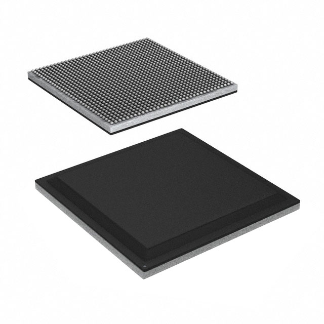
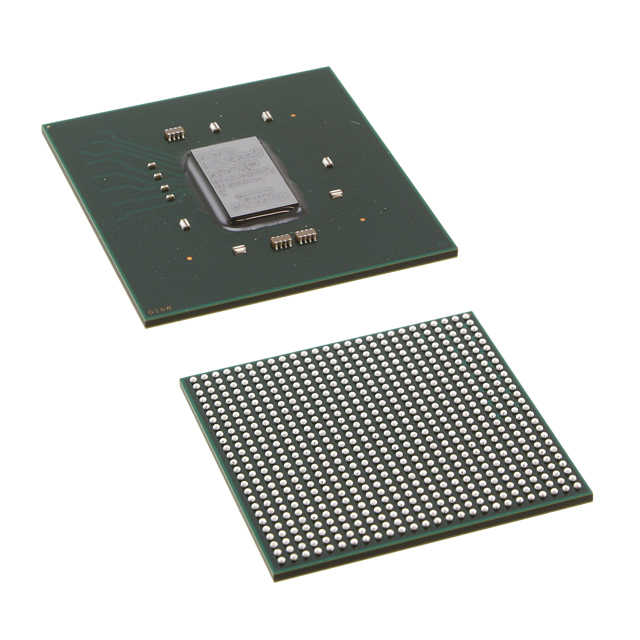
Kintex® UltraScale™ Field Programmable Gate Array (FPGA) IC 312 13004800 318150 1156-BBGA, FCBGA |
|---|---|
| Quantity | 732 Available (as of October 8, 2026) |
| Product Category | Field Programmable Gate Array (FPGA) |
|---|---|
| Manufacturer | AMD |
| Manufacturing Status | Active |
| Manufacturer Standard Lead Time | 16 Weeks |
| Datasheet |
Specifications & Environmental
| Device Package | 1156-FCBGA (35x35) | Grade | Commercial | Operating Temperature | 0°C – 85°C | ||
|---|---|---|---|---|---|---|---|
| Package / Case | 1156-BBGA, FCBGA | Number of I/O | 312 | Voltage | 922 mV - 979 mV | ||
| Mounting Method | Surface Mount | RoHS Compliance | ROHS3 Compliant | REACH Compliance | REACH Unaffected | ||
| Moisture Sensitivity Level | 4 (72 Hours) | Number of LABs/CLBs | 18180 | Number of Logic Elements/Cells | 318150 | ||
| Number of Gates | N/A | ECCN | 3A991D | HTS Code | 8542.39.0001 | ||
| Qualification | N/A | Total RAM Bits | 13004800 |
Overview of XCKU025-1FFVA1156C – Kintex® UltraScale™ FPGA IC, 1156-FCBGA
The XCKU025-1FFVA1156C is a Kintex® UltraScale™ field programmable gate array (FPGA) packaged in a 1156-FCBGA (35×35) surface-mount ball grid array. It provides substantial programmable logic capacity, embedded memory, and a high I/O count intended for FPGA-based designs that require flexible digital implementation and system integration.
With approximately 318,150 logic elements and roughly 13 Mbits of on‑chip RAM, this commercial‑grade device balances logic density, memory, and I/O resources for a wide range of custom digital designs operating within a 0 °C to 85 °C temperature range and a core supply range of 922 mV to 979 mV.
Key Features
- Core Logic Capacity Approximately 318,150 logic elements enable implementation of complex combinational and sequential logic functions within a single FPGA device.
- Embedded Memory Approximately 13 Mbits of on‑chip RAM provide local storage for buffering, FIFOs, and memory‑mapped logic structures.
- I/O Resources 312 user I/Os allow broad external connectivity for sensors, peripherals, and board‑level interfaces.
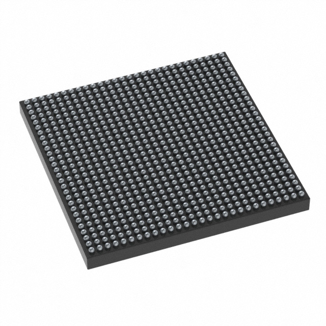
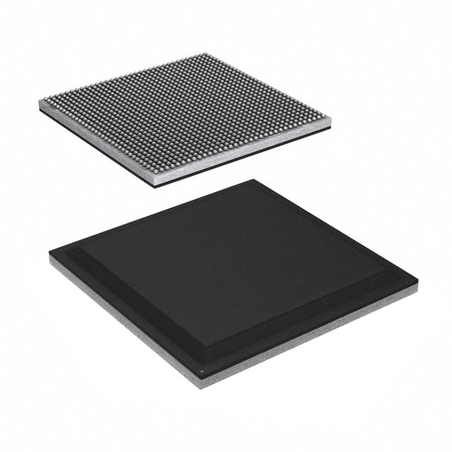
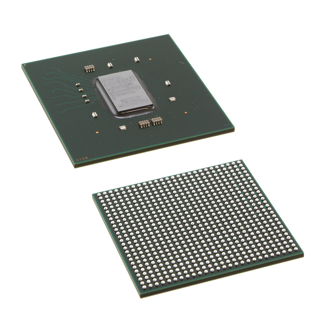
- Package & Mounting 1156‑ball FCBGA (35×35) surface‑mount package offers high interconnect density for compact board designs.
- Power Supply Range Core voltage operation between 922 mV and 979 mV supports targeted power domains and system-level power planning.
- Operating Temperature Commercial grade operation from 0 °C to 85 °C for standard ambient environments.
- Standards Compliance RoHS compliant construction supports environmental regulation requirements for many markets.
Typical Applications
- Custom digital logic and prototyping Use the device’s logic capacity and embedded RAM to develop and validate tailored digital architectures and IP cores.
- Hardware acceleration Leverage abundant logic elements and on‑chip memory to offload compute‑intensive algorithms into programmable fabric.
- High‑density I/O integration Take advantage of 312 I/Os for consolidating multiple peripheral interfaces and system-level interconnects on a single FPGA.
Unique Advantages
- Substantial logic resources: Approximately 318,150 logic elements provide the headroom to implement large custom logic designs without immediate need for multi‑device partitioning.
- Meaningful on‑chip memory: Roughly 13 Mbits of embedded RAM reduce reliance on external memory for buffering and state storage, simplifying board routing and BOM.
- High I/O count: 312 user I/Os enable flexible system integration and connectivity to a wide range of peripherals and interfaces.
- Compact, high-density package: The 1156‑ball FCBGA (35×35) package supports dense board layouts while retaining high interconnect capability.
- Commercial temperature rating: Rated for 0 °C to 85 °C operation to match standard commercial applications and environments.
- RoHS compliant: Environmentally compliant construction simplifies design for regulated markets.
Why Choose XCKU025-1FFVA1156C?
The XCKU025-1FFVA1156C positions itself as a balanced Kintex® UltraScale™ FPGA option for designers who need a combination of significant logic capacity, embedded memory, and a high number of I/Os in a compact FCBGA package. Its commercial temperature rating and RoHS compliance make it suitable for standard embedded and OEM applications where those attributes are required.
This device is appropriate for engineering teams and product developers implementing mid‑to‑large scale programmable logic, on‑chip buffering, and dense board integration while maintaining predictable power and thermal planning based on the provided supply and operating temperature specifications.
Request a quote or submit an inquiry to obtain pricing, availability, and ordering information for the XCKU025-1FFVA1156C.





















Date Founded: 1969
Headquarters: Santa Clara, California, USA
Employees: 25,000+
Revenue: $22.68 Billion
Certifications and Memberships: ISO9001:2015, RoHS, REACH











