
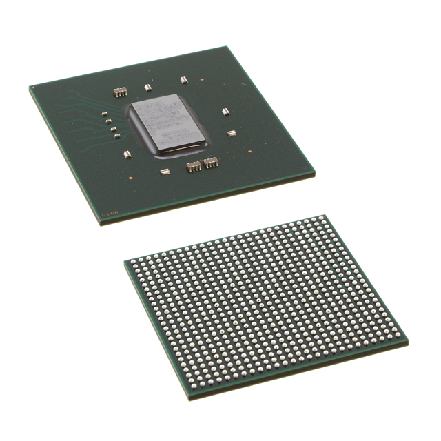
XCKU040-1FFVA1156I
| Part Description |
Kintex® UltraScale™ Field Programmable Gate Array (FPGA) IC 520 21606000 530250 1156-BBGA, FCBGA |
|---|---|
| Quantity | 516 Available (as of June 15, 2026) |

| Product Category | Field Programmable Gate Array (FPGA) |
|---|---|
| Manufacturer | AMD |
| Manufacturing Status | Active |
| Manufacturer Standard Lead Time | 16 Weeks |
| Datasheet |
Specifications & Environmental
| Device Package | 1156-FCBGA (35x35) | Grade | Industrial | Operating Temperature | -40°C – 100°C | ||
|---|---|---|---|---|---|---|---|
| Package / Case | 1156-BBGA, FCBGA | Number of I/O | 520 | Voltage | 922 mV - 979 mV | ||
| Mounting Method | Surface Mount | RoHS Compliance | ROHS3 Compliant | REACH Compliance | REACH Unaffected | ||
| Moisture Sensitivity Level | 4 (72 Hours) | Number of LABs/CLBs | 30300 | Number of Logic Elements/Cells | 530250 | ||
| Number of Gates | N/A | ECCN | 3A991D | HTS Code | 8542.39.0001 | ||
| Qualification | N/A | Total RAM Bits | 21606000 |
Overview of XCKU040-1FFVA1156I – Kintex® UltraScale™ FPGA, 1156-FCBGA (520 I/O)
The XCKU040-1FFVA1156I is a Kintex® UltraScale™ field programmable gate array (FPGA) from AMD, packaged in a 1156-FCBGA (35×35) surface-mount package. It delivers a large fabric of programmable logic and embedded memory suitable for designs that require significant on‑chip resources and high I/O counts.
With 530,250 logic elements, approximately 21.606 Mbits of embedded memory, and 520 I/O pins, this industrial‑grade device targets applications that need substantial integration of logic, memory, and peripheral connectivity within a single FPGA footprint.
Key Features
- Programmable Logic Capacity — Contains 530,250 logic elements organized across 30,300 CLBs to implement complex digital logic and custom accelerators.
- Embedded Memory — Total on‑chip RAM of 21,606,000 bits (approximately 21.606 Mbits) for buffering, lookup tables, and state storage within the FPGA fabric.
- I/O Density — 520 I/O pins to support extensive peripheral connectivity and multiple high‑pin-count interfaces.
- Package — 1156-BBGA / 1156-FCBGA (35×35) supplier device package designed for surface-mount PCB assembly.
- Power Supply Range — Core supply operating range specified at 922 mV to 979 mV for the device core domain.
- Industrial Temperature Grade — Rated for operation from -40 °C to 100 °C to meet a broad set of environmental conditions.
- Mounting — Surface-mount assembly suitable for standard PCB manufacturing processes.
Typical Applications
- High‑density digital processing — Use the large logic element count and CLB resources to implement SIMD datapaths, custom state machines, and protocol processing within a single device.
- Memory‑rich buffering — Leverage approximately 21.606 Mbits of embedded memory for frame buffers, packet queues, or large on‑chip FIFOs.
- Multi‑interface systems — The 520 I/O pins support designs that require numerous external connections, sensor interfaces, or parallel data buses.
Unique Advantages
- Substantial logic fabric: 530,250 logic elements and 30,300 CLBs offer the scale needed to merge multiple functions onto one FPGA, reducing board-level component count.
- Significant on‑chip memory: Approximately 21.606 Mbits of embedded RAM allow designers to implement large buffers and state storage without external memory for many use cases.
- High I/O capacity: 520 available I/O pins enable complex interconnections and support for multiple parallel interfaces or sensors from a single package.
- Industrial temperature range: Rated from -40 °C to 100 °C to address applications that operate across wide ambient conditions.
- Standard surface‑mount package: The 1156-FCBGA (35×35) package supports established PCB assembly processes and dense board layouts.
Why Choose XCKU040-1FFVA1156I?
The XCKU040-1FFVA1156I positions itself as a high‑capacity Kintex® UltraScale™ FPGA option for engineers who need a balance of logic, embedded memory, and abundant I/O in a single industrial‑grade, surface‑mount package. Its combination of 530,250 logic elements, approximately 21.606 Mbits of on‑chip RAM, and 520 I/O makes it suitable for consolidating multiple functional blocks and reducing system BOM complexity.
Designed for customers developing complex digital systems, the device provides a scalable hardware platform for prototyping and deployment where ample programmable resources and a broad operating temperature range are required.
Request a quote or submit your design requirements to receive pricing and availability for the XCKU040-1FFVA1156I.


Date Founded: 1969
Headquarters: Santa Clara, California, USA
Employees: 25,000+
Revenue: $22.68 Billion
Certifications and Memberships: ISO9001:2015, RoHS, REACH


