
XCKU040-2FBVA900I
| Part Description |
Kintex® UltraScale™ Field Programmable Gate Array (FPGA) IC 468 21606000 530250 900-BBGA, FCBGA |
|---|---|
| Quantity | 1,182 Available (as of June 14, 2026) |
| Product Category | Field Programmable Gate Array (FPGA) |
|---|---|
| Manufacturer | AMD |
| Manufacturing Status | Active |
| Manufacturer Standard Lead Time | 16 Weeks |
| Datasheet |
Specifications & Environmental
| Device Package | 900-FCBGA (31x31) | Grade | Industrial | Operating Temperature | -40°C – 100°C | ||
|---|---|---|---|---|---|---|---|
| Package / Case | 900-BBGA, FCBGA | Number of I/O | 468 | Voltage | 922 mV - 979 mV | ||
| Mounting Method | Surface Mount | RoHS Compliance | ROHS3 Compliant | REACH Compliance | REACH Unaffected | ||
| Moisture Sensitivity Level | 4 (72 Hours) | Number of LABs/CLBs | 30300 | Number of Logic Elements/Cells | 530250 | ||
| Number of Gates | N/A | ECCN | 3A991D | HTS Code | 8542.39.0001 | ||
| Qualification | N/A | Total RAM Bits | 21606000 |
Overview of XCKU040-2FBVA900I – Kintex® UltraScale™ Field Programmable Gate Array IC, 900-FCBGA (31×31), Industrial
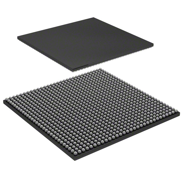
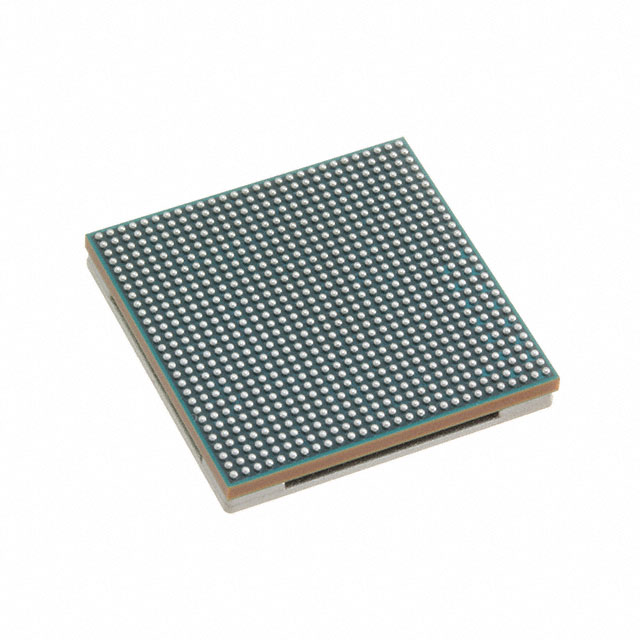
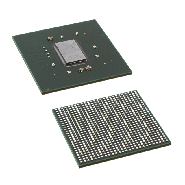
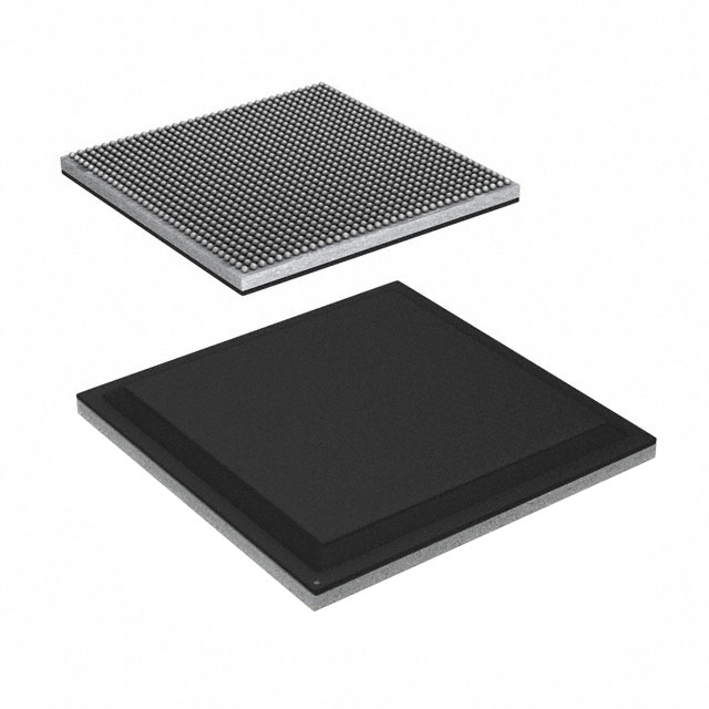
The XCKU040-2FBVA900I is a Kintex® UltraScale™ field programmable gate array (FPGA) IC from AMD. It integrates a large array of configurable logic with on-chip memory and a broad I/O complement in a 900-ball FCBGA package for surface-mount assembly.
Key on-chip resources include 530,250 logic elements, approximately 21.6 Mbits of embedded memory, 30,300 CLBs, and 468 I/O pins. The device is specified for industrial operation with a supply range of 922 mV to 979 mV and an operating temperature range of −40 °C to 100 °C.
Key Features
- Core Logic 530,250 logic elements provide a large programmable fabric for custom digital functions and complex digital signal processing.
- Configurable Logic Blocks (CLBs) 30,300 CLBs available for building scalable, parallel logic architectures and control logic implementations.
- Embedded Memory Approximately 21.6 Mbits of on-chip RAM to support buffering, lookup tables, and application-specific memory needs without external DRAM for many use cases.
- I/O Count 468 I/O pins support wide parallel interfaces, multiple serial lanes, or mixed-signal front ends when combined with external PHYs or transceivers.
- Package & Mounting 900-ball FCBGA (31×31) package designed for surface-mount assembly to facilitate compact board layouts and high-density system integration.
- Power Supply Specified core supply range of 922 mV to 979 mV for the device core domain.
- Temperature & Grade Industrial-grade device rated for operation from −40 °C to 100 °C to meet extended-temperature system requirements.
- Environmental Compliance RoHS compliant, supporting regulatory requirements for lead-free manufacturing.
Unique Advantages
- High logic density: 530,250 logic elements enable consolidation of multiple functions into a single device, reducing board count and interconnect complexity.
- Substantial embedded memory: Approximately 21.6 Mbits of on-chip RAM minimizes dependence on external memory for many buffering and LUT needs, simplifying board design.
- Large I/O capacity: 468 I/Os allow flexible interfacing with sensors, ADC/DAC front ends, and high-bandwidth parallel or serialized data paths.
- Industrial temperature rating: Specified −40 °C to 100 °C operation supports deployment in environments requiring extended-temperature reliability.
- Compact FCBGA footprint: 900-ball, 31×31 FCBGA provides a compact, high-density package for space-constrained system designs.
- Regulatory readiness: RoHS compliance simplifies adoption in lead-free manufacturing processes.
Why Choose XCKU040-2FBVA900I?
The XCKU040-2FBVA900I combines a substantial programmable logic fabric with significant on-chip memory and a high I/O count in a 900-FCBGA package suited for surface-mount integration. Its industrial temperature rating and defined core supply range make it a practical choice for designs that require robust operation across extended temperatures and precise power domains.
This device is well suited to designers and system engineers who need to integrate complex digital logic, memory-intensive functions, and numerous external interfaces into a single FPGA platform while maintaining a compact board footprint and compliance with RoHS requirements.
Request a quote or submit an inquiry for pricing and availability of XCKU040-2FBVA900I to evaluate the device for your next design.


Date Founded: 1969
Headquarters: Santa Clara, California, USA
Employees: 25,000+
Revenue: $22.68 Billion
Certifications and Memberships: ISO9001:2015, RoHS, REACH


