
XCKU040-2FFVA1156E
| Part Description |
Kintex® UltraScale™ Field Programmable Gate Array (FPGA) IC 520 21606000 530250 1156-BBGA, FCBGA |
|---|---|
| Quantity | 198 Available (as of June 14, 2026) |

| Product Category | Field Programmable Gate Array (FPGA) |
|---|---|
| Manufacturer | AMD |
| Manufacturing Status | Active |
| Manufacturer Standard Lead Time | 16 Weeks |
| Datasheet |
Specifications & Environmental
| Device Package | 1156-FCBGA (35x35) | Grade | Extended | Operating Temperature | 0°C – 100°C | ||
|---|---|---|---|---|---|---|---|
| Package / Case | 1156-BBGA, FCBGA | Number of I/O | 520 | Voltage | 922 mV - 979 mV | ||
| Mounting Method | Surface Mount | RoHS Compliance | ROHS3 Compliant | REACH Compliance | REACH Unaffected | ||
| Moisture Sensitivity Level | 4 (72 Hours) | Number of LABs/CLBs | 30300 | Number of Logic Elements/Cells | 530250 | ||
| Number of Gates | N/A | ECCN | 3A991D | HTS Code | 8542.39.0001 | ||
| Qualification | N/A | Total RAM Bits | 21606000 |
Overview of XCKU040-2FFVA1156E – Kintex® UltraScale™ Field Programmable Gate Array (FPGA) IC
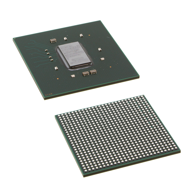
The XCKU040-2FFVA1156E is a Kintex® UltraScale™ field programmable gate array optimized for high-density logic and I/O‑intensive board‑level implementations. It integrates a large logic fabric, substantial on‑chip RAM, and a high I/O count in a 1156‑ball FCBGA package to support complex digital designs.
Targeted at applications that require significant programmable logic capacity and numerous external interfaces, this device delivers a combination of logic resources, embedded memory, and I/O count suitable for demanding FPGA-based systems while operating within a supply range of 922 mV to 979 mV and an extended temperature grade.
Key Features
- Core / Logic — 530,250 logic elements (logic cells) to implement large, performance-oriented designs.
- Configurable Logic Blocks (CLBs) — 30,300 CLBs for structured logic partitioning and design scalability.
- Embedded Memory — Approximately 21.6 Mbits of on‑chip RAM for data buffering, state storage, and algorithm working memory.
- I/O Density — 520 user I/Os to support wide parallel interfaces and mixed-signal front ends.
- Power — Operates from a core supply range of 922 mV to 979 mV to match system power architectures.
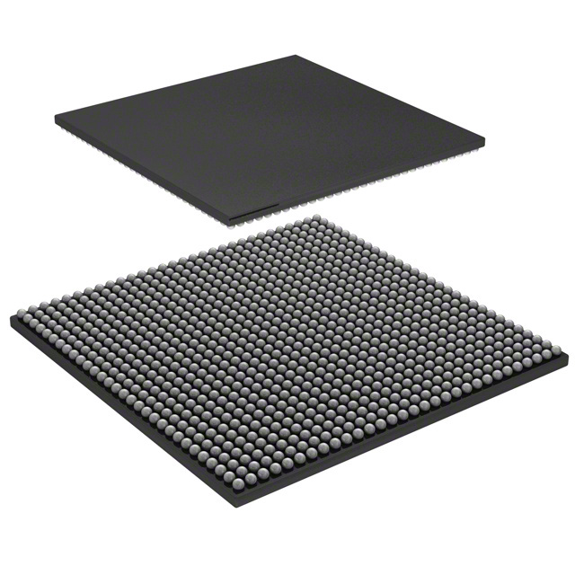
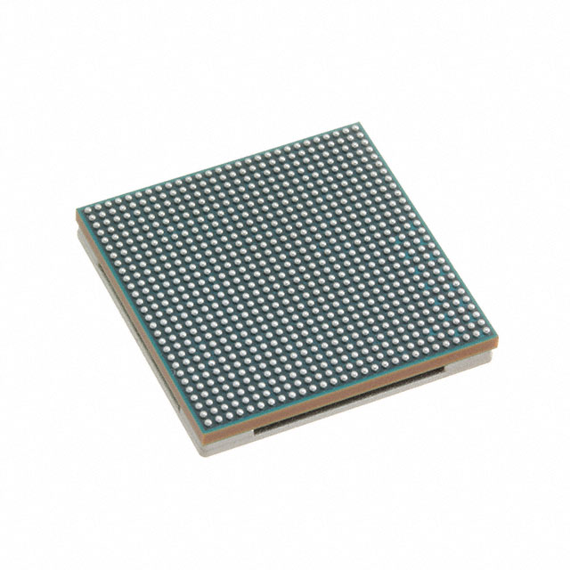
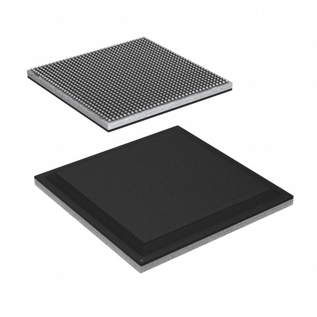
- Package & Mounting — 1156‑BBGA / 1156‑FCBGA supplier package (35 × 35 mm) in a surface‑mount form factor for board‑level integration.
- Temperature & Grade — Extended grade with an operating temperature range of 0 °C to 100 °C for broader deployment environments.
- Environmental Compliance — RoHS compliant for global electronics manufacturing requirements.
Typical Applications
- High‑density signal processing — Implement complex DSP and custom logic algorithms using the large logic element count and embedded memory.
- I/O‑rich communication systems — Support multiple high‑speed and parallel interfaces with 520 available I/Os.
- Custom hardware accelerators — Deploy application‑specific acceleration blocks that leverage the device’s logic capacity and on‑chip RAM.
- Board‑level FPGA modules — Integrate as the programmable heart of single-board systems requiring a compact 1156‑ball FCBGA solution.
Unique Advantages
- Large programmable fabric: 530,250 logic elements and 30,300 CLBs enable mapping of substantial digital designs without immediate partitioning across multiple devices.
- Significant on‑chip memory: Approximately 21.6 Mbits of embedded RAM reduces dependence on external memory for many buffering and state‑storage tasks.
- High I/O availability: 520 I/Os simplify board routing for multi‑channel and parallel interface requirements, reducing the need for external I/O expanders.
- Compact FCBGA package: The 1156‑ball FCBGA (35 × 35 mm) package combines density with surface‑mount assembly for modern PCB designs.
- Extended operational range: Grade: Extended and 0 °C to 100 °C operating temperature accommodates a wider set of deployment conditions.
- Compliance‑ready: RoHS compliance supports responsible manufacturing and supply chain requirements.
Why Choose XCKU040-2FFVA1156E?
The XCKU040-2FFVA1156E positions itself as a scalable, high‑capacity FPGA for designs that demand extensive logic resources, substantial embedded memory, and a large number of external interfaces. Its 1156‑ball FCBGA package and surface‑mount mounting make it suitable for compact, board‑level implementations where density and I/O count matter.
This device is well suited for engineering teams building compute‑intensive or I/O‑centric systems who need a balance of logic capacity, on‑chip RAM, and integration readiness. Its extended grade and RoHS compliance support longer deployment cycles and modern manufacturing requirements.
If you require pricing, availability, or detailed ordering information, request a quote or submit a product inquiry to receive assistance and the latest supply details.


Date Founded: 1969
Headquarters: Santa Clara, California, USA
Employees: 25,000+
Revenue: $22.68 Billion
Certifications and Memberships: ISO9001:2015, RoHS, REACH


