
XCKU040-L1FBVA676I
| Part Description |
Kintex® UltraScale™ Field Programmable Gate Array (FPGA) IC 312 21606000 530250 676-BBGA, FCBGA |
|---|---|
| Quantity | 825 Available (as of June 14, 2026) |

| Product Category | Field Programmable Gate Array (FPGA) |
|---|---|
| Manufacturer | AMD |
| Manufacturing Status | Active |
| Manufacturer Standard Lead Time | 16 Weeks |
| Datasheet |
Specifications & Environmental
| Device Package | 676-FCBGA (27x27) | Grade | Industrial | Operating Temperature | -40°C – 100°C | ||
|---|---|---|---|---|---|---|---|
| Package / Case | 676-BBGA, FCBGA | Number of I/O | 312 | Voltage | 880 mV - 979 mV | ||
| Mounting Method | Surface Mount | RoHS Compliance | ROHS3 Compliant | REACH Compliance | REACH Unaffected | ||
| Moisture Sensitivity Level | 4 (72 Hours) | Number of LABs/CLBs | 30300 | Number of Logic Elements/Cells | 530250 | ||
| Number of Gates | N/A | ECCN | 3A991D | HTS Code | 8542.39.0001 | ||
| Qualification | N/A | Total RAM Bits | 21606000 |
Overview of XCKU040-L1FBVA676I – Kintex® UltraScale™ Field Programmable Gate Array (FPGA)
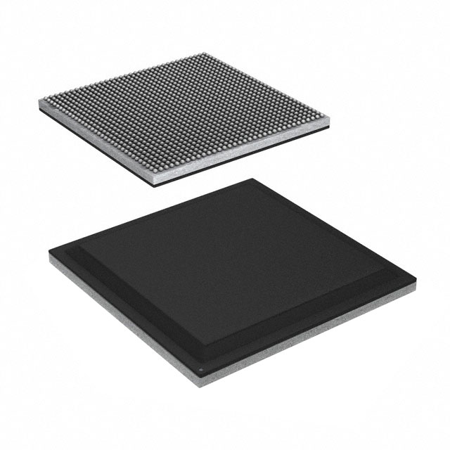
The XCKU040-L1FBVA676I is a Kintex® UltraScale™ field programmable gate array (FPGA) IC from AMD, supplied in a 676-ball FCBGA package. It is an industrial-grade device that combines a large logic fabric, significant on-chip memory, and a substantial I/O count for demanding embedded and control-oriented designs.
Key differentiators visible in the datasheet entry include 530,250 logic elements, approximately 21.6 Mbits of embedded memory, and 312 I/Os, all delivered in a compact 676-FCBGA (27×27) surface-mount package with an operating range from −40 °C to 100 °C.
Key Features
- Core Logic Contains 530,250 logic elements, providing a large programmable fabric for implementing complex digital functions and custom logic.
- Embedded Memory Approximately 21.6 Mbits of on-chip RAM, enabling local buffering, state storage, and data-path acceleration without external memory for many use cases.
- I/O Capacity 312 I/Os to support wide peripheral connectivity, parallel interfaces, and multi-channel signal routing directly at the FPGA boundary.
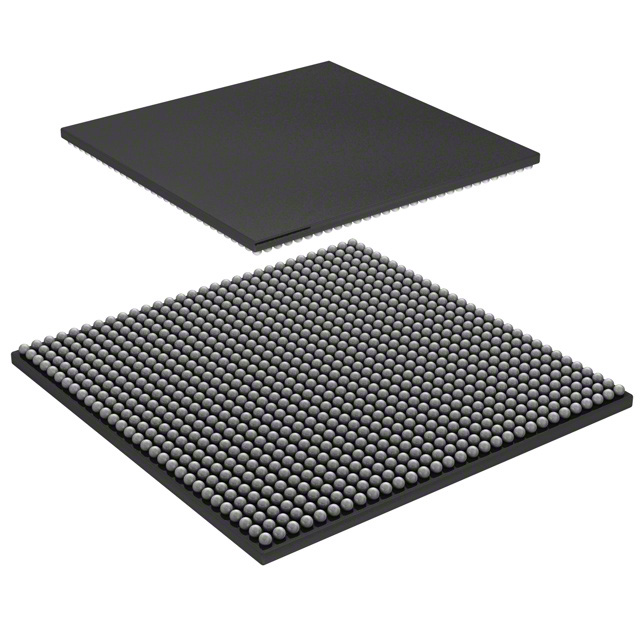
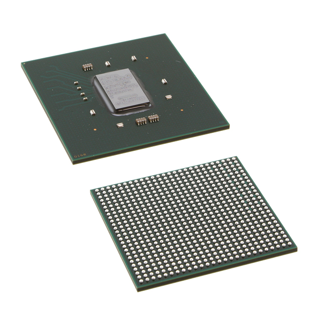
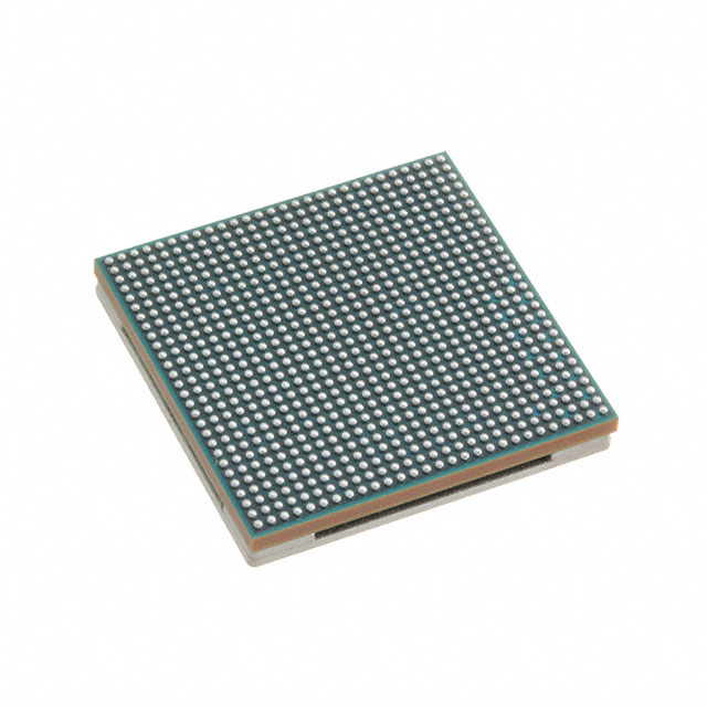
- Package & Mounting 676-BBGA, FCBGA package with supplier device package 676-FCBGA (27×27); designed for surface-mount assembly to fit dense PCB layouts.
- Power Specified operating supply range from 880 mV to 979 mV, enabling designers to plan supply rails and power sequencing around the device requirements.
- Temperature & Grade Industrial-grade operation with an ambient range of −40 °C to 100 °C, suitable for extended-temperature deployments.
- Regulatory Compliance RoHS compliant, supporting lead-free manufacturing and environmental compliance goals.
Typical Applications
- Industrial control and automation The industrial-grade temperature range and substantial I/O count make this FPGA suitable for control-system logic, I/O aggregation, and deterministic processing in industrial environments.
- High-density digital processing With 530,250 logic elements and ~21.6 Mbits of embedded memory, the device supports complex data-path implementations and custom acceleration blocks.
- Embedded system integration The combination of on-chip RAM, large logic capacity, and numerous I/Os enables system designers to consolidate functions and reduce external component count in embedded platforms.
Unique Advantages
- Large programmable fabric: 530,250 logic elements provide room for extensive custom logic, allowing complex algorithms and parallel processing structures to be implemented on-chip.
- Significant on-chip memory: Approximately 21.6 Mbits of embedded RAM reduce reliance on external memory for many buffering and working-set requirements.
- Extensive I/O connectivity: 312 I/Os support broad peripheral interfacing and multiple parallel lanes, simplifying board-level routing for multi-channel designs.
- Compact, industry-ready package: 676-FCBGA (27×27) surface-mount package provides a dense solution for space-constrained PCBs while maintaining high pin count.
- Industrial operating range: Rated from −40 °C to 100 °C for deployments that require extended temperature resilience.
- RoHS compliant: Meets lead-free manufacturing and environmental compliance requirements for modern production processes.
Why Choose XCKU040-L1FBVA676I?
The XCKU040-L1FBVA676I positions itself as an industrial-grade Kintex® UltraScale™ FPGA that combines a large logic element count, substantial embedded memory, and a high peripheral I/O count in a compact 676-FCBGA package. These attributes make it appropriate for designs that need significant on-chip resources and broad connectivity while operating across an extended temperature range.
Manufactured by AMD and offered in a surface-mount FCBGA, this device is suitable for engineering teams and procurement groups targeting industrial applications that require dense programmable logic, local memory capacity, and a high-pin-count package for system consolidation.
Request a quote or submit a procurement inquiry to begin evaluation and obtain pricing and availability for the XCKU040-L1FBVA676I.


Date Founded: 1969
Headquarters: Santa Clara, California, USA
Employees: 25,000+
Revenue: $22.68 Billion
Certifications and Memberships: ISO9001:2015, RoHS, REACH


