
XCKU060-1FFVA1156I
| Part Description |
Kintex® UltraScale™ Field Programmable Gate Array (FPGA) IC 520 38912000 725550 1156-BBGA, FCBGA |
|---|---|
| Quantity | 764 Available (as of June 15, 2026) |

| Product Category | Field Programmable Gate Array (FPGA) |
|---|---|
| Manufacturer | AMD |
| Manufacturing Status | Active |
| Manufacturer Standard Lead Time | 16 Weeks |
| Datasheet |
Specifications & Environmental
| Device Package | 1156-FCBGA (35x35) | Grade | Industrial | Operating Temperature | -40°C – 100°C | ||
|---|---|---|---|---|---|---|---|
| Package / Case | 1156-BBGA, FCBGA | Number of I/O | 520 | Voltage | 922 mV - 979 mV | ||
| Mounting Method | Surface Mount | RoHS Compliance | ROHS3 Compliant | REACH Compliance | REACH Unaffected | ||
| Moisture Sensitivity Level | 4 (72 Hours) | Number of LABs/CLBs | 41460 | Number of Logic Elements/Cells | 725550 | ||
| Number of Gates | N/A | ECCN | 3A991D | HTS Code | 8542.39.0001 | ||
| Qualification | N/A | Total RAM Bits | 38912000 |
Overview of XCKU060-1FFVA1156I – Kintex® UltraScale™ FPGA, 520 I/O, 1156-FCBGA
The XCKU060-1FFVA1156I is a Kintex® UltraScale™ field programmable gate array (FPGA) IC from AMD in a 1156-ball FCBGA package. It delivers a high density of programmable logic and on-chip memory with a large I/O complement, targeting industrial applications that require significant logic capacity and flexible I/O integration.
Key Features
- Core Logic 725,550 logic elements provide substantial programmable logic capacity for complex custom hardware acceleration and control functions.
- Embedded Memory Approximately 39 Mbits of on-chip RAM support large buffering, lookup tables and state storage without external memory.
- I/O Capability 520 I/O pins enable extensive peripheral and interface connectivity for multi-channel systems and dense board-level integration.
- Power Core supply range of 0.922 V to 0.979 V for the device core power domain as specified.
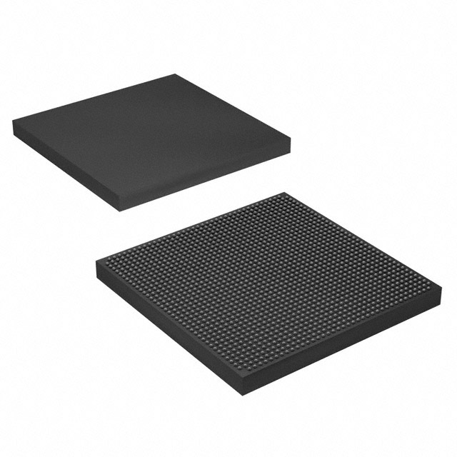
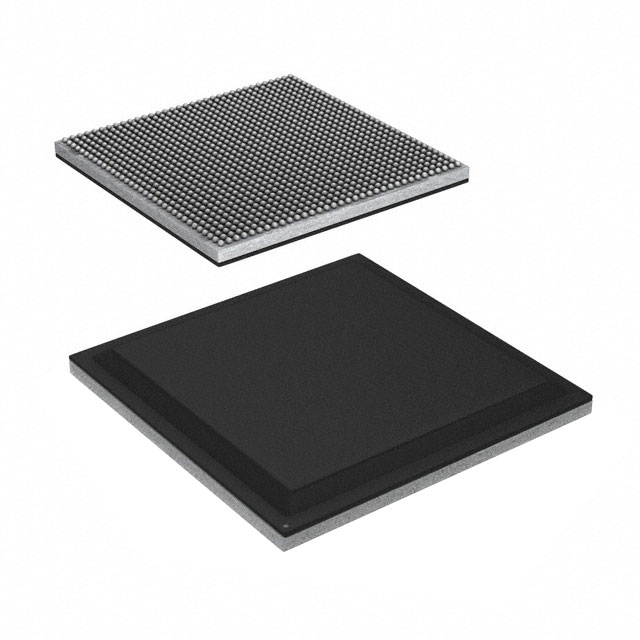
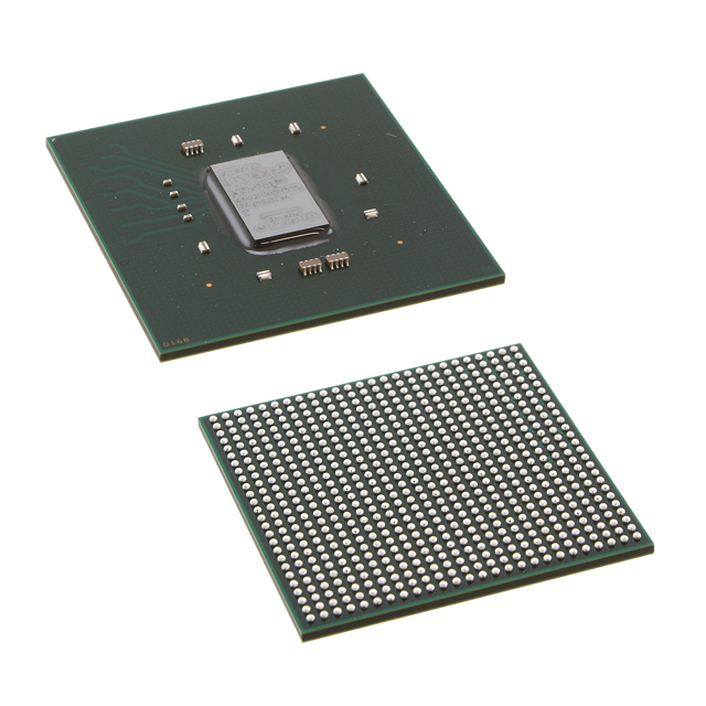
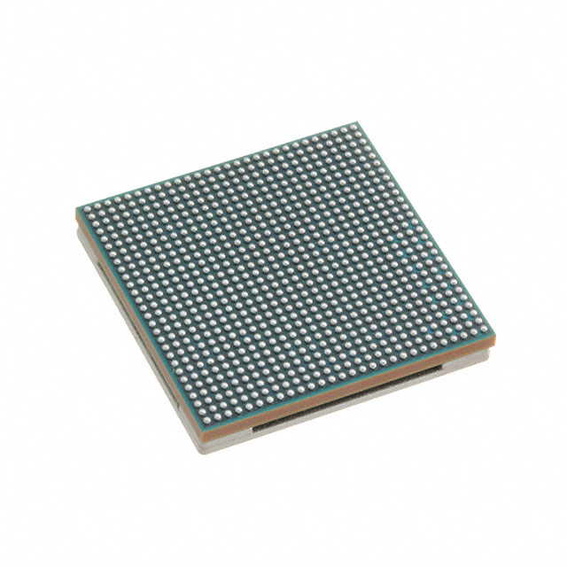
- Package & Mounting 1156-ball FCBGA (35 × 35 mm) surface-mount package for compact, board-level deployment and high pin-count routing.
- Operating Temperature & Grade Rated for industrial operation from −40 °C to 100 °C and specified as industrial grade.
- Environmental Compliance RoHS-compliant to meet common environmental and manufacturing requirements.
Unique Advantages
- High logic density: 725,550 logic elements allow consolidation of complex functions into a single FPGA, reducing system component count.
- Significant on‑chip memory: Approximately 39 Mbits of embedded RAM supports large buffers and state machines without immediate dependence on external memory.
- Extensive I/O: 520 I/O pins provide flexibility for multi-protocol interfaces and high-channel-count designs.
- Industrial temperature range: −40 °C to 100 °C rating supports deployment in demanding temperature environments.
- Compact high‑pin package: 1156‑FCBGA (35 × 35 mm) enables dense routing and high pin-count connectivity in a manageable footprint.
- RoHS compliant: Aligns with common environmental requirements for electronics manufacturing.
Why Choose XCKU060-1FFVA1156I?
The XCKU060-1FFVA1156I combines a large logic element count, substantial embedded memory and a high I/O count in a compact 1156-ball FCBGA package, offering a balanced platform for designs that require on‑chip capacity and extensive connectivity. Its industrial temperature rating and RoHS compliance make it suitable for long‑lifecycle and environmentally conscious projects.
This device is well suited for engineers and procurement teams looking for a high‑capacity, industrial‑grade FPGA to consolidate functions, reduce BOM complexity, and provide a scalable foundation for advanced digital designs.
Request a quote or submit an inquiry to receive pricing and availability information for the XCKU060-1FFVA1156I and to discuss how this FPGA can fit your design requirements.


Date Founded: 1969
Headquarters: Santa Clara, California, USA
Employees: 25,000+
Revenue: $22.68 Billion
Certifications and Memberships: ISO9001:2015, RoHS, REACH


