
XCKU040-L1SFVA784I
| Part Description |
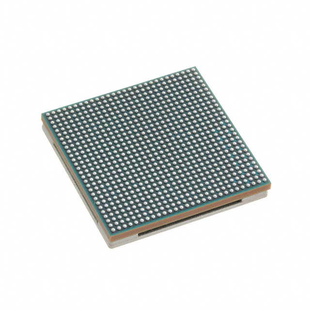
Kintex® UltraScale™ Field Programmable Gate Array (FPGA) IC 468 21606000 530250 784-BFBGA, FCCSP |
|---|---|
| Quantity | 159 Available (as of June 14, 2026) |
| Product Category | Field Programmable Gate Array (FPGA) |
|---|---|
| Manufacturer | AMD |
| Manufacturing Status | Active |
| Manufacturer Standard Lead Time | 16 Weeks |
| Datasheet |
Specifications & Environmental
| Device Package | 784-FCCSPBGA (23x23) | Grade | Industrial | Operating Temperature | -40°C – 100°C | ||
|---|---|---|---|---|---|---|---|
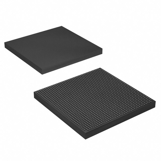
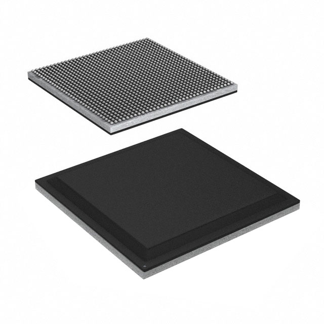
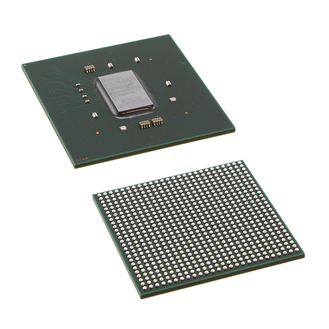
| Package / Case | 784-BFBGA, FCCSP | Number of I/O | 468 | Voltage | 880 mV - 979 mV | ||
| Mounting Method | Surface Mount | RoHS Compliance | ROHS3 Compliant | REACH Compliance | REACH Unaffected | ||
| Moisture Sensitivity Level | 4 (72 Hours) | Number of LABs/CLBs | 30300 | Number of Logic Elements/Cells | 530250 | ||
| Number of Gates | N/A | ECCN | 3A991D | HTS Code | 8542.39.0001 | ||
| Qualification | N/A | Total RAM Bits | 21606000 |
Overview of XCKU040-L1SFVA784I – Kintex® UltraScale™ FPGA IC, 530,250 Logic Elements
The XCKU040-L1SFVA784I is a Kintex® UltraScale™ Field Programmable Gate Array (FPGA) IC from AMD, supplied in a 784-BFBGA / FCCSP package. It provides a high density of programmable logic and embedded memory in a surface-mount package targeted for industrial applications requiring robust operation across a wide temperature range.
With hundreds of user I/Os, a large pool of logic elements and on-chip RAM, this device suits designs that demand substantial parallel processing, complex control logic, and dense I/O interfacing while operating at low core voltages.
Key Features
- Logic Capacity – Approximately 530,250 logic elements, enabling large-scale programmable logic implementations and complex digital algorithms.
- Configurable Logic Blocks – High logical resource count for partitioning functions and implementing parallel datapaths.
- Embedded Memory – Approximately 21.6 Mbits of on-chip RAM for buffering, lookup tables, and local data storage.
- I/O Density – 468 user I/Os to support broad peripheral and bus interfacing requirements.
- Package & Mounting – 784-BFBGA, FCCSP package; supplier device package listed as 784-FCCSPBGA (23x23). Surface-mount device for PCB integration.
- Power – Core supply range from 880 mV to 979 mV for low-voltage operation.
- Industrial Temperature Range – Rated for operation from -40°C to 100°C to meet demanding environmental conditions.
- Manufacturer – Produced by AMD, providing a recognizable supplier pedigree.
Typical Applications
- Industrial Control and Automation – Implements complex control logic and state machines while withstanding industrial temperature ranges.
- High-Density I/O Systems – Interfaces numerous sensors, actuators, and parallel buses using its 468 user I/Os.
- Signal Processing and Data Aggregation – Uses large logic capacity and ~21.6 Mbits of embedded memory for buffering and parallel processing pipelines.
- Embedded System Prototyping – Provides ample logic and memory resources for validating hardware accelerators and custom controllers.
Unique Advantages
- High Logic Density: Approximately 530,250 logic elements allow integration of complex functions that reduce external component count.
- Substantial Embedded Memory: Around 21.6 Mbits of on-chip RAM supports local data storage, reducing reliance on off-chip memory.
- Extensive I/O Capability: 468 user I/Os enable broad connectivity to peripherals, buses and sensors in dense system designs.
- Industrial Reliability: Rated for -40°C to 100°C operation, suitable for harsh environmental deployments.
- Compact, Surface-Mount Packaging: 784-BFBGA / 784-FCCSPBGA (23x23) package balances density and board-level integration for space-constrained designs.
- Low-Voltage Core Operation: 880 mV to 979 mV supply range supports modern low-power system architectures.
Why Choose XCKU040-L1SFVA784I?
The XCKU040-L1SFVA784I positions itself as a high-capacity, industrial-grade FPGA choice for designers who need significant programmable logic, ample embedded memory and a large I/O footprint in a compact surface-mount package. Its electrical and thermal specifications are targeted at robust, long-lived deployments where environmental tolerance and high integration matter.
Ideal for engineers developing industrial control, signal processing, and complex I/O systems, this AMD Kintex® UltraScale™ device provides the resources to consolidate functions, reduce BOM complexity, and scale designs as requirements evolve.
If you would like pricing or availability information, request a quote or submit an RFQ detailing quantities and delivery requirements to receive a prompt response.


Date Founded: 1969
Headquarters: Santa Clara, California, USA
Employees: 25,000+
Revenue: $22.68 Billion
Certifications and Memberships: ISO9001:2015, RoHS, REACH


