
XCKU115-2FLVA2104I
| Part Description |
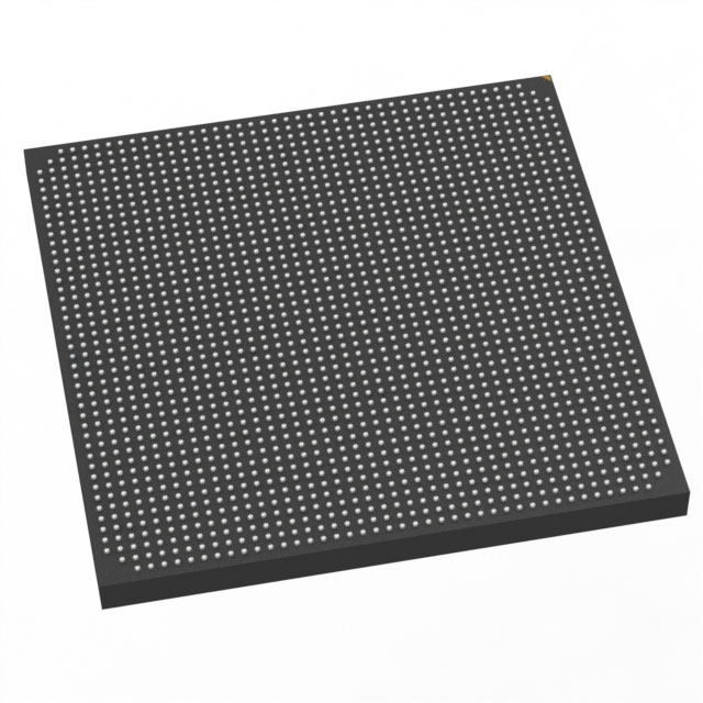
Kintex® UltraScale™ Field Programmable Gate Array (FPGA) IC 832 77721600 1451100 2104-BBGA, FCBGA |
|---|---|
| Quantity | 500 Available (as of June 15, 2026) |

| Product Category | Field Programmable Gate Array (FPGA) |
|---|---|
| Manufacturer | AMD |
| Manufacturing Status | Active |
| Manufacturer Standard Lead Time | 20 Weeks |
| Datasheet |
Specifications & Environmental
| Device Package | 2104-FCBGA (47.5x47.5) | Grade | Industrial | Operating Temperature | -40°C – 100°C | ||
|---|---|---|---|---|---|---|---|
| Package / Case | 2104-BBGA, FCBGA | Number of I/O | 832 | Voltage | 922 mV - 979 mV | ||
| Mounting Method | Surface Mount | RoHS Compliance | ROHS3 Compliant | REACH Compliance | REACH Unaffected | ||
| Moisture Sensitivity Level | 4 (72 Hours) | Number of LABs/CLBs | 82920 | Number of Logic Elements/Cells | 1451100 | ||
| Number of Gates | N/A | ECCN | 3A001A7B | HTS Code | 8542.39.0001 | ||
| Qualification | N/A | Total RAM Bits | 77721600 |
Overview of XCKU115-2FLVA2104I – Kintex® UltraScale™ FPGA, 2104-FCBGA (Industrial)
The XCKU115-2FLVA2104I is a Kintex® UltraScale™ field programmable gate array (FPGA) IC from AMD designed for high‑density programmable logic applications. It combines a large logic fabric with substantial on‑chip memory and a high I/O count in a 2104‑ball FCBGA surface‑mount package targeted at industrial environments.
This device is positioned for designs requiring significant logic capacity, on‑chip RAM and broad interfacing capability while supporting industrial temperature operation and a defined core voltage supply range.
Key Features
- Core Logic Approximately 1,451,100 logic elements provide substantial programmable logic resources for complex digital designs.
- Embedded Memory Approximately 78 Mbits of on‑chip RAM support large buffering, data staging and memory‑intensive algorithms.
- High I/O Count 832 user I/O pins enable extensive connectivity to peripherals, high‑speed interfaces and multi‑lane systems.
- Power Specified core supply range of 922 mV to 979 mV for predictable power planning and regulation design.
- Package & Mounting 2104‑ball FCBGA (47.5 × 47.5 mm) surface‑mount package provides a compact, high‑pin‑count footprint for board integration.
- Operating Range Industrial operating temperature from −40 °C to 100 °C for deployment in temperature‑challenging environments.
- Manufacturer Built by AMD as part of the Kintex® UltraScale™ family.
- RoHS Compliance RoHS compliant for environmental and regulatory planning.
Typical Applications
- High‑density digital signal processing Large logic capacity and substantial on‑chip memory support DSP pipelines, algorithm acceleration and complex data paths.
- Interface aggregation and bridging 832 I/O pins accommodate multi‑lane interfaces, protocol bridging and wide peripheral connectivity on a single device.
- Industrial control and automation Industrial temperature rating and surface‑mount packaging make the device suitable for factory automation and control systems requiring robust programmable logic.
- System prototyping and integration High logic element count and embedded RAM allow system architects to prototype large, integrated FPGA‑based designs.
Unique Advantages
- Highly integrated logic capacity: Over one million logic elements enable consolidation of complex functions into a single FPGA, reducing BOM and board complexity.
- Significant embedded memory: Approximately 78 Mbits of on‑chip RAM provide room for buffering, state storage and data‑intensive processing without external memory.
- Extensive I/O availability: 832 I/O pins support wide interfacing options and simplify multi‑channel or multi‑protocol implementations.
- Industrial temperature support: Specified operation from −40 °C to 100 °C helps ensure reliable operation in demanding industrial environments.
- Compact, high‑pin‑count package: The 2104‑FCBGA (47.5 × 47.5 mm) package delivers high connectivity in a space‑efficient footprint for dense board designs.
- Defined power envelope: A clear core supply range (922 mV–979 mV) aids in power supply planning and thermal analysis.
Why Choose XCKU115-2FLVA2104I?
The XCKU115-2FLVA2104I offers a balance of very high logic density, large embedded memory and extensive I/O in an industrial‑rated Kintex® UltraScale™ device from AMD. Its combination of resources and package density makes it well suited for complex FPGA designs that require consolidation of functions, significant on‑chip buffering and broad external connectivity.
Designers targeting industrial automation, high‑throughput digital processing or large‑scale prototyping will find this device provides the core resources and operating range needed for robust system implementation and scalability within the Kintex® UltraScale™ family.
Request a quote or submit an inquiry to receive pricing, availability and ordering information for the XCKU115-2FLVA2104I.


Date Founded: 1969
Headquarters: Santa Clara, California, USA
Employees: 25,000+
Revenue: $22.68 Billion
Certifications and Memberships: ISO9001:2015, RoHS, REACH


