
XCKU115-2FLVB2104I
| Part Description |
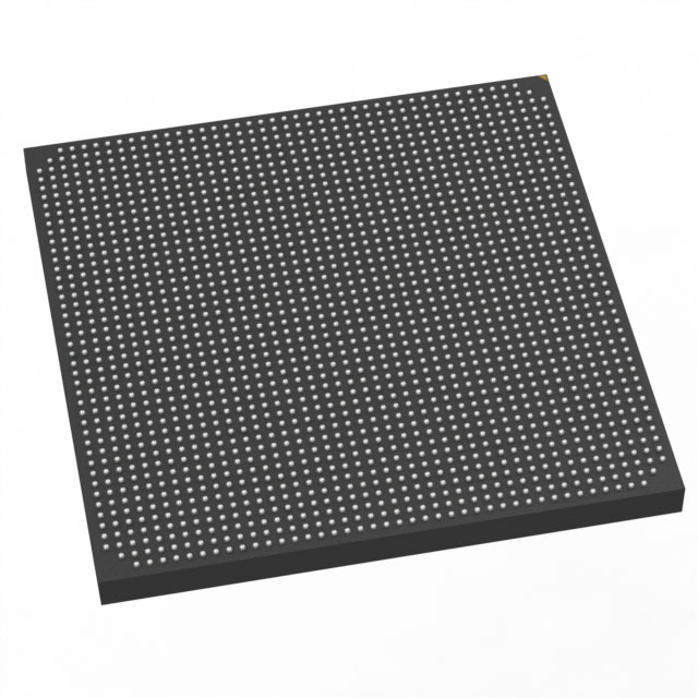
Kintex UltraScale FPGA, XCKU115, 1,451,000 Logic Cells, 5520 DSP, FLVB2104, Commercial |
|---|---|
| Quantity | 803 Available (as of June 14, 2026) |

| Product Category | Field Programmable Gate Array (FPGA) |
|---|---|
| Manufacturer | AMD |
| Manufacturing Status | Active |
| Manufacturer Standard Lead Time | 20 Weeks |
| Datasheet |
Specifications & Environmental
| Device Package | FLVB2104 | Grade | N/A | Operating Temperature | -40°C – 100°C | ||
|---|---|---|---|---|---|---|---|
| Package / Case | 2104-BGA | Number of I/O | 832 | Voltage | 922 mV - 979 mV | ||
| Mounting Method | Surface Mount | RoHS Compliance | Compliant | REACH Compliance | REACH Unaffected | ||
| Moisture Sensitivity Level | 4 | Number of LABs/CLBs | 663360 | Number of Logic Elements/Cells | 1451000 | ||
| Number of Gates | N/A | ECCN | EAR99 | HTS Code | 8542.31.00.60 | ||
| Qualification | N/A | Total RAM Bits | 79586918 |
Overview of XCKU115-2FLVB2104I – Kintex® UltraScale™ FPGA, 2104-FCBGA (47.5×47.5), Industrial
The XCKU115-2FLVB2104I is a Kintex® UltraScale™ field programmable gate array (FPGA) from AMD designed for complex, high-density digital designs. It provides a high count of logic elements, substantial on-chip memory, and a large I/O complement in a 2104-FCBGA surface-mount package intended for industrial applications.
Key Features
- Core FPGA Architecture Kintex® UltraScale™ FPGA family architecture implemented in this device for large-scale programmable logic integration.
- Logic Capacity Approximately 1,451,100 logic elements to support complex combinational and sequential logic implementations.
- Embedded Memory Approximately 77.7 Mbits of embedded memory for buffering, LUT-based storage, and on-chip data handling.
- I/O Density 702 user I/O pins to support high-density interfacing and system-level connectivity.
- Package and Mounting 2104-FCBGA package (47.5×47.5 mm), surface-mount design suitable for compact board integration.
- Power Supply Range Core supply range of 0.922–0.979 V to match tight power-domain requirements.
- Industrial Temperature Range Rated for operation from -40 °C to 100 °C to meet industrial-environment thermal requirements.
- Regulatory Compliance RoHS compliant to support regulatory requirements for lead-free manufacturing.
Typical Applications
- High-density interface systems Use the 702 I/Os to aggregate and route numerous external interfaces in communication or data-acquisition designs.
- Large-scale logic implementations Leverage ~1.45M logic elements for complex control, processing, and signal-flow architectures.
- Memory-intensive FPGA functions Utilize ~77.7 Mbits of on-chip memory for packet buffering, frame storage, and large LUT-based structures.
- Industrial control and automation Industrial-grade temperature range and surface-mount packaging make this device suitable for industrial system controllers and automation equipment.
Unique Advantages
- High logic integration: Approximately 1,451,100 logic elements enable consolidation of multi-chip logic into a single FPGA, reducing BOM and board complexity.
- Substantial embedded memory: Approximately 77.7 Mbits of on-chip RAM supports large buffers and data-path acceleration without depending on external memory.
- Extensive I/O capacity: 702 I/Os provide flexibility for dense peripheral connectivity and multi-channel designs.
- Industrial-rated thermal range: -40 °C to 100 °C operating range addresses the thermal demands of industrial environments.
- Compact FCBGA package: The 2104-FCBGA (47.5×47.5 mm) offers high pin count in a compact form factor for space-constrained designs.
- Controlled core voltage: Narrow supply window (0.922–0.979 V) supports predictable power-domain behavior for tightly managed systems.
Why Choose XCKU115-2FLVB2104I?
The XCKU115-2FLVB2104I positions itself for designs that require high logic density, substantial on-chip memory, and a large number of I/Os in an industrial-rated FPGA package. Its combination of approximately 1.45M logic elements, ~77.7 Mbits of embedded RAM, and 702 I/Os enables consolidation of complex functions while reducing external component count.
Backed by AMD's Kintex® UltraScale™ portfolio, this device is suited to engineers and procurement teams building robust industrial systems that need scalable logic resources, high I/O counts, and a compact FCBGA footprint.
Request a quote or submit an inquiry to obtain pricing, availability, and ordering information for XCKU115-2FLVB2104I.


Date Founded: 1969
Headquarters: Santa Clara, California, USA
Employees: 25,000+
Revenue: $22.68 Billion
Certifications and Memberships: ISO9001:2015, RoHS, REACH


