
XCKU115-2FLVF1924I
| Part Description |
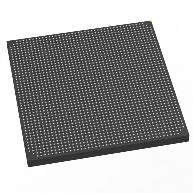
Kintex® UltraScale™ Field Programmable Gate Array (FPGA) IC 728 77721600 1451100 1924-BBGA, FCBGA |
|---|---|
| Quantity | 948 Available (as of June 15, 2026) |

| Product Category | Field Programmable Gate Array (FPGA) |
|---|---|
| Manufacturer | AMD |
| Manufacturing Status | Active |
| Manufacturer Standard Lead Time | 20 Weeks |
| Datasheet |
Specifications & Environmental
| Device Package | 1924-FCBGA (45x45) | Grade | Industrial | Operating Temperature | -40°C – 100°C | ||
|---|---|---|---|---|---|---|---|
| Package / Case | 1924-BBGA, FCBGA | Number of I/O | 728 | Voltage | 922 mV - 979 mV | ||
| Mounting Method | Surface Mount | RoHS Compliance | ROHS3 Compliant | REACH Compliance | REACH Unknown | ||
| Moisture Sensitivity Level | 4 (72 Hours) | Number of LABs/CLBs | 82920 | Number of Logic Elements/Cells | 1451100 | ||
| Number of Gates | N/A | ECCN | 3A001A7B | HTS Code | 8542.39.0001 | ||
| Qualification | N/A | Total RAM Bits | 77721600 |
Overview of XCKU115-2FLVF1924I – Kintex® UltraScale™ FPGA, 1924‑FCBGA (Industrial)
The XCKU115-2FLVF1924I is a Kintex® UltraScale™ field programmable gate array (FPGA) IC from AMD. This device delivers a very large programmable fabric with 1,451,100 logic elements, approximately 77.7 Mbits of embedded memory, and 728 user I/O pins in a 1924‑FCBGA package.
Specified for industrial use with a surface‑mount 1924‑FCBGA (45×45) package and an operating range of -40 °C to 100 °C, the device is intended for designs that require high integration density, substantial on‑chip RAM, and a large number of I/O connections. Supply voltage is specified between 922 mV and 979 mV.
Key Features
- Logic Capacity — 1,451,100 logic elements to implement large-scale programmable logic, custom datapaths, and parallel processing functions.
- Embedded Memory — Approximately 77.7 Mbits of on‑chip RAM for buffering, look‑up tables, and memory‑intensive algorithms without external memory dependency.
- I/O Density — 728 user I/O pins to support numerous interfaces, parallel buses, and high‑pin‑count system connections.
- Package and Mounting — 1924‑BBGA / 1924‑FCBGA package (supplier package: 1924‑FCBGA 45×45) in a surface‑mount form factor for compact board layout and high pin‑count routing.
- Power — Specified supply voltage range from 922 mV to 979 mV to match system power rails and regulator designs.
- Operating Range — Industrial temperature rating from -40 °C to 100 °C for deployment in thermally demanding environments.
- Manufacturer — Produced by AMD and provided in a form factor suited to high‑density FPGA deployments.
- Standards — RoHS compliant, supporting environmental regulations for lead‑free assembly.
Typical Applications
- High‑density digital processing — Use the 1,451,100 logic elements and substantial embedded memory to implement complex algorithms, wide parallel datapaths, and custom hardware accelerators.
- Multi‑interface aggregation — The 728 I/O pins accommodate numerous serial and parallel interfaces, sensor arrays, or multiport connectivity on a single device.
- On‑board buffering and memory‑intensive logic — Approximately 77.7 Mbits of embedded RAM supports large FIFOs, packet buffering, and temporary data storage without immediate need for external memory.
Unique Advantages
- Extensive programmable fabric: 1,451,100 logic elements allow designers to consolidate multiple functions into a single device, reducing BOM complexity.
- Significant on‑chip memory: Approximately 77.7 Mbits of embedded RAM enables large local storage for improved data throughput and lower external memory dependence.
- High I/O count: 728 user I/Os provide flexibility to interface directly with many peripherals and system buses, simplifying board-level architecture.
- Industrial temperature range: Rated from -40 °C to 100 °C to support deployments where extended ambient temperatures are expected.
- Compact, high‑pin package: 1924‑FCBGA (45×45) surface‑mount package supports dense PCB routing while maintaining robust mechanical mounting.
- RoHS compliant: Conforms to environmental lead‑free requirements for modern electronic assembly processes.
Why Choose XCKU115-2FLVF1924I?
The XCKU115-2FLVF1924I positions itself as a high‑capacity, highly integrated FPGA option for designs that demand large programmable logic resources, abundant embedded memory, and extensive I/O connectivity. Its industrial temperature rating and surface‑mount 1924‑FCBGA package make it suitable for compact, robust system designs requiring long‑term stability.
Designed and manufactured by AMD, this Kintex® UltraScale™ device provides a combination of logic density, on‑chip RAM, and I/O scalability that supports complex, evolving projects—enabling consolidation of functions and potential reductions in system BOM and board complexity.
Request a quote or submit an inquiry for pricing and availability of the XCKU115-2FLVF1924I to evaluate its fit for your next design.


Date Founded: 1969
Headquarters: Santa Clara, California, USA
Employees: 25,000+
Revenue: $22.68 Billion
Certifications and Memberships: ISO9001:2015, RoHS, REACH


