
XCKU115-L1FLVA1517I
| Part Description |
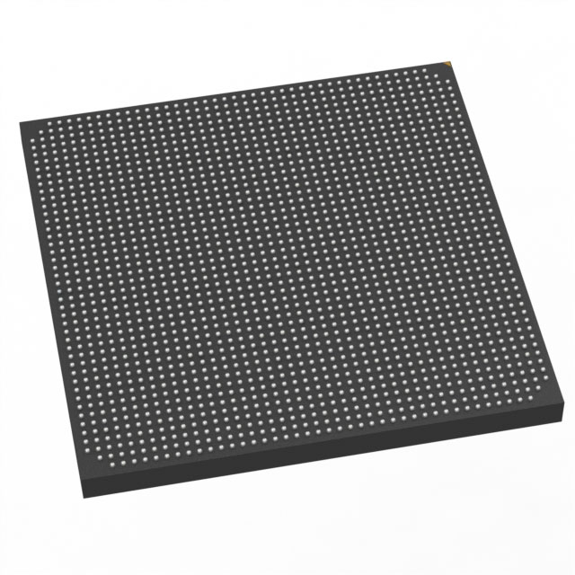
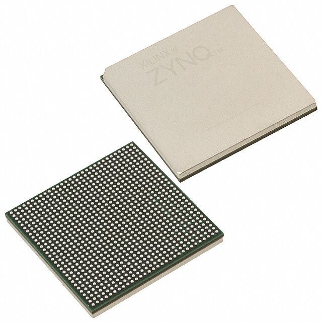
Kintex® UltraScale™ Field Programmable Gate Array (FPGA) IC 624 77721600 1451100 1517-BBGA, FCBGA |
|---|---|
| Quantity | 5 Available (as of June 17, 2026) |

| Product Category | Field Programmable Gate Array (FPGA) |
|---|---|
| Manufacturer | AMD |
| Manufacturing Status | Active |
| Manufacturer Standard Lead Time | 20 Weeks |
| Datasheet |
Specifications & Environmental
| Device Package | 1517-FCBGA (40x40) | Grade | Industrial | Operating Temperature | -40°C – 100°C | ||
|---|---|---|---|---|---|---|---|
| Package / Case | 1517-BBGA, FCBGA | Number of I/O | 624 | Voltage | 880 mV - 979 mV | ||
| Mounting Method | Surface Mount | RoHS Compliance | ROHS3 Compliant | REACH Compliance | REACH Unaffected | ||
| Moisture Sensitivity Level | 2A (4 Weeks) | Number of LABs/CLBs | 82920 | Number of Logic Elements/Cells | 1451100 | ||
| Number of Gates | N/A | ECCN | 3A001A7B | HTS Code | 8542.39.0001 | ||
| Qualification | N/A | Total RAM Bits | 77721600 |
Overview of XCKU115-L1FLVA1517I – Kintex® UltraScale™ FPGA, 1517-FCBGA (Industrial)
The XCKU115-L1FLVA1517I is a Kintex® UltraScale™ Field Programmable Gate Array (FPGA) in a 1517-FCBGA package designed for high-density, programmable logic applications. It offers a combination of large logic capacity, substantial embedded memory, and a high I/O count for projects that require significant on-chip resources.
Targets include systems that need extensive programmable logic and memory close to the data path while operating across an industrial temperature range. Key value comes from its logic density, embedded memory capacity, and flexible I/O in a compact surface-mount FCBGA package.
Key Features
- High Logic Capacity Approximately 1,451,100 logic elements to implement large-scale logic, control, and processing functions on-chip.
- Embedded Memory Approximately 77.7 Mbits of on-chip RAM for buffering, packet processing, and memory-intensive algorithms.
- I/O Density 624 user I/O pins to support wide parallel interfaces, multiple high-pin-count peripherals, and complex board-level connectivity.
- Package and Mounting 1517-FCBGA (1517-BBGA) package with a 40 × 40 mm footprint, designed for surface-mount assembly to minimize board area while providing high pin count.
- Power Supply Range Core voltage supply range of 880 mV to 979 mV to match system power-rail designs and regulator selections.
- Industrial Temperature Grade Specified for operation from −40 °C to 100 °C to meet demanding environmental requirements.
- RoHS Compliant Manufactured in compliance with RoHS directives for lead-free assembly and regulatory alignment.
Typical Applications
- Data and Packet Processing: Implement high-throughput packet engines and protocol offloads using large logic and embedded memory for buffering and histogramming.
- Signal Processing and Acceleration: Deploy FPGA-based accelerators for compute-intensive algorithms that benefit from on-chip RAM and dense logic integration.
- Telecommunications and Networking: Build line cards, switching fabrics, and interface bridges that require many I/Os and extensive programmable logic.
- Industrial Control Systems: Use the industrial temperature rating and robust I/O count for complex control, monitoring, and automation tasks in harsh environments.
- High-Density Prototyping: Validate large FPGA designs and system architectures that need significant on-chip resources before volume implementation.
Unique Advantages
- Highly integrated logic and memory: Combines approximately 1.45 million logic elements with about 77.7 Mbits of embedded RAM to reduce external memory dependency and board-level complexity.
- Extensive I/O capability: 624 user I/Os provide flexibility to interface with multiple high-pin-count peripherals and parallel buses without external expanders.
- Industrial operating range: Rated from −40 °C to 100 °C to support deployments in temperature-challenging environments.
- Compact, high-pin-count package: 1517-FCBGA (40 × 40 mm) enables high integration density while keeping board footprint manageable.
- Controlled core voltage range: 880 mV to 979 mV core supply specification simplifies power-supply design and regulator selection.
- Regulatory alignment: RoHS compliance supports lead-free manufacturing and regulatory requirements.
Why Choose XCKU115-L1FLVA1517I?
The XCKU115-L1FLVA1517I delivers a balance of high logic density, substantial embedded memory, and large I/O capacity in a compact FCBGA package rated for industrial temperatures. It is suitable for designers building complex programmable systems that require on-chip resources and robust environmental performance.
This device is appropriate for development teams and production systems that prioritize integration and scalability—enabling consolidation of functions onto a single FPGA die while maintaining practical board-level design choices and compliance with RoHS requirements.
Request a quote or submit a pricing inquiry to get availability and ordering information for the XCKU115-L1FLVA1517I.


Date Founded: 1969
Headquarters: Santa Clara, California, USA
Employees: 25,000+
Revenue: $22.68 Billion
Certifications and Memberships: ISO9001:2015, RoHS, REACH


