
XCKU11P-1FFVE1517E
| Part Description |
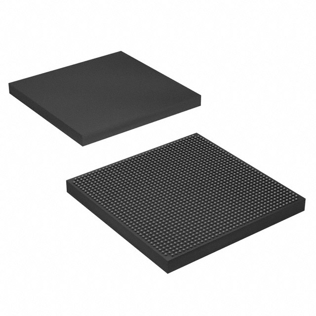
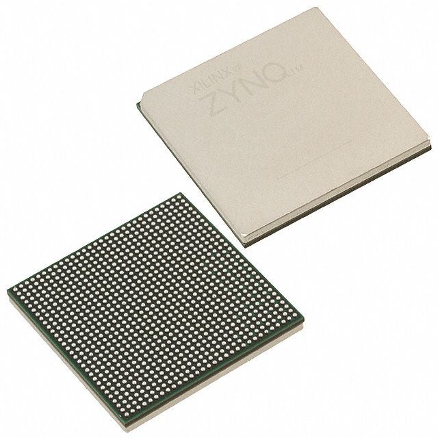
Kintex® UltraScale+™ Field Programmable Gate Array (FPGA) IC 512 53964800 653100 1517-BBGA, FCBGA |
|---|---|
| Quantity | 1,240 Available (as of June 18, 2026) |
| Product Category | Field Programmable Gate Array (FPGA) |
|---|---|
| Manufacturer | AMD |
| Manufacturing Status | Active |
| Manufacturer Standard Lead Time | 16 Weeks |
| Datasheet |
Specifications & Environmental
| Device Package | 1517-FCBGA (40x40) | Grade | Extended | Operating Temperature | 0°C – 100°C | ||
|---|---|---|---|---|---|---|---|
| Package / Case | 1517-BBGA, FCBGA | Number of I/O | 512 | Voltage | 825 mV - 876 mV | ||
| Mounting Method | Surface Mount | RoHS Compliance | ROHS3 Compliant | REACH Compliance | REACH Unknown | ||
| Moisture Sensitivity Level | 4 (72 Hours) | Number of LABs/CLBs | 37320 | Number of Logic Elements/Cells | 653100 | ||
| Number of Gates | N/A | ECCN | 3A001A7B | HTS Code | 8542.39.0001 | ||
| Qualification | N/A | Total RAM Bits | 53964800 |
Overview of XCKU11P-1FFVE1517E – Kintex® UltraScale+™ Field Programmable Gate Array (FPGA)
The XCKU11P-1FFVE1517E is a Kintex® UltraScale+™ Field Programmable Gate Array (FPGA) IC from AMD. It delivers a high on-chip resource set including logic, embedded memory, and I/O in a 1517-ball FCBGA package for surface-mount integration. This device is specified with an extended grade operating range and low-voltage core supply, suitable for designs that require significant programmable logic capacity, embedded memory, and a large I/O complement.
Key Features
- Core Logic — 653,100 logic elements and 37,320 CLBs provide substantial programmable logic capacity for complex digital designs.
- Embedded Memory — Approximately 54 Mbits of on-chip RAM to support large buffers, FIFOs, and data storage close to logic.
- I/O Count — 512 user I/O pins for wide-ranging interface requirements and parallel connectivity.
- Power Supply — Core voltage supply range of 825 mV to 876 mV for the device core.
- Package & Mounting — 1517-BBGA (1517-FCBGA, 40×40) package in a surface-mount form factor for compact board-level integration.
- Temperature & Grade — Extended grade with an operating temperature range of 0 °C to 100 °C.
- Regulatory — RoHS compliant.
Unique Advantages
- High logic capacity: 653,100 logic elements enable implementation of large-scale, highly parallel architectures without external programmable logic.
- Substantial embedded memory: Approximately 54 Mbits of on-chip RAM reduces dependence on external memory for intermediate data storage.
- Extensive I/O resources: 512 I/O pins provide flexibility for multiple interfaces and broad system connectivity.
- Compact FCBGA package: The 1517-FCBGA (40×40) package supports dense integration on modern PCBs while maintaining a surface-mount footprint.
- Low-voltage core operation: Core supply between 825 mV and 876 mV aligns with low-voltage system designs.
- Extended operating range: Rated for 0 °C to 100 °C operation and provided in an extended grade for broader environmental use cases.
Why Choose XCKU11P-1FFVE1517E?
The XCKU11P-1FFVE1517E balances a large programmable logic fabric with significant embedded memory and a high I/O count in a compact 1517-FCBGA package. Its combination of 653,100 logic elements, approximately 54 Mbits of on-chip RAM, and 512 I/Os makes it well suited for complex FPGA-based systems that demand integrated resources and board-level density.
Designed and supplied by AMD, this Kintex® UltraScale+™ device provides a clear upgrade path for projects that need substantial programmable capacity while maintaining a compact footprint and extended-grade temperature operation. It is a practical choice for engineering teams seeking scalable, high-resource FPGAs with surface-mount packaging.
Request a quote or submit a pricing inquiry to get availability and lead-time information for the XCKU11P-1FFVE1517E.


Date Founded: 1969
Headquarters: Santa Clara, California, USA
Employees: 25,000+
Revenue: $22.68 Billion
Certifications and Memberships: ISO9001:2015, RoHS, REACH


