
XCKU11P-L2FFVE1517E
| Part Description |
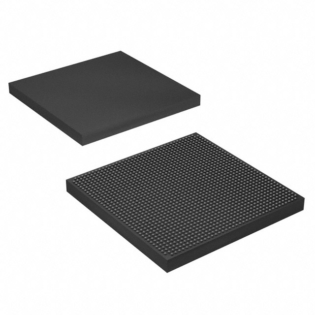
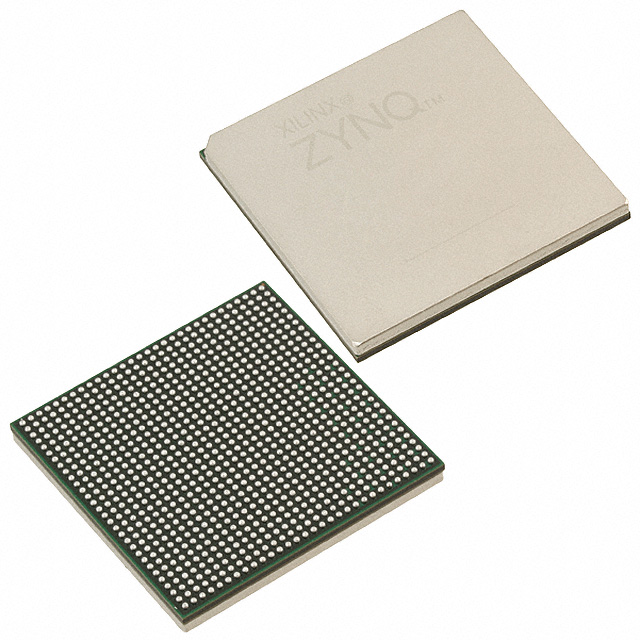
Kintex® UltraScale+™ Field Programmable Gate Array (FPGA) IC 512 53964800 653100 1517-BBGA, FCBGA |
|---|---|
| Quantity | 365 Available (as of June 15, 2026) |
| Product Category | Field Programmable Gate Array (FPGA) |
|---|---|
| Manufacturer | AMD |
| Manufacturing Status | Active |
| Manufacturer Standard Lead Time | 16 Weeks |
| Datasheet |
Specifications & Environmental
| Device Package | 1517-FCBGA (40x40) | Grade | Extended | Operating Temperature | 0°C – 100°C | ||
|---|---|---|---|---|---|---|---|
| Package / Case | 1517-BBGA, FCBGA | Number of I/O | 512 | Voltage | 698 mV - 876 mV | ||
| Mounting Method | Surface Mount | RoHS Compliance | ROHS3 Compliant | REACH Compliance | REACH Unknown | ||
| Moisture Sensitivity Level | 4 (72 Hours) | Number of LABs/CLBs | 37320 | Number of Logic Elements/Cells | 653100 | ||
| Number of Gates | N/A | ECCN | 5A002A1 | HTS Code | 8542.39.0001 | ||
| Qualification | N/A | Total RAM Bits | 53964800 |
Overview of XCKU11P-L2FFVE1517E – Kintex® UltraScale+™ FPGA, 653,100 logic elements
The XCKU11P-L2FFVE1517E is a Kintex® UltraScale+™ field programmable gate array (FPGA) designed for high-density programmable logic applications. It integrates a large logic fabric, significant on-chip memory, and a broad I/O count in a 1517-FCBGA package to support complex digital designs.
With 653,100 logic elements, approximately 54 Mbits of embedded memory, and 512 I/O, this device is targeted at designs that require high logic capacity, substantial local memory, and extensive external connectivity while maintaining a compact surface-mount package footprint.
Key Features
- Core Architecture Kintex® UltraScale+™ FPGA fabric providing 653,100 logic elements for implementing complex programmable logic.
- Embedded Memory Approximately 54 Mbits of on-chip RAM to support data buffering, packet buffering, and local storage needs without external memory in some use cases.
- I/O Capacity 512 user I/O pins to interface with a wide range of external devices and high-pin-count systems.
- Power Supply Operates with core supply voltage in the range of 698 mV to 876 mV, enabling compatibility with targeted system power architectures.
- Package & Mounting 1517-FCBGA (1517-BBGA) surface-mount package, supplier package size 1517-FCBGA (40×40) for compact board-level integration.
- Temperature & Grade Extended-grade device rated for operation from 0 °C to 100 °C.
- Regulatory RoHS compliant, supporting regulatory requirements for lead-free assemblies.
Typical Applications
- High-density logic systems Implement complex programmable logic and custom processing functions using the device's 653,100 logic elements and substantial embedded memory.
- Data buffering and local storage Use the approximately 54 Mbits of on-chip RAM for packet buffering, FIFO implementations, and latency-sensitive data staging.
- I/O-intensive designs Leverage 512 I/O pins to connect to multiple peripherals, sensors, or interface subsystems on compact PCB layouts.
Unique Advantages
- Large programmable fabric: 653,100 logic elements provide the capacity to consolidate multiple functions into a single device, reducing board-level component count.
- Substantial embedded memory: Approximately 54 Mbits of on-chip RAM reduces reliance on external memory for many buffering and storage needs, simplifying design and improving performance.
- High I/O density: 512 I/O pins enable broad connectivity for multi-channel systems and complex peripheral integration without multiple interface chips.
- Compact FCBGA packaging: 1517-FCBGA (40×40) surface-mount package balances high pin count with a compact board footprint for space-constrained designs.
- Extended temperature rating: 0 °C to 100 °C operation supports deployment in thermally demanding applications within the specified range.
- RoHS compliant: Meets lead-free assembly requirements for modern electronics manufacturing.
Why Choose XCKU11P-L2FFVE1517E?
The XCKU11P-L2FFVE1517E positions itself as a high-capacity, highly integrated Kintex UltraScale+ FPGA option for designs that require substantial logic resources, on-chip memory, and extensive I/O in a compact FCBGA package. Its combination of 653,100 logic elements, approximately 54 Mbits of embedded memory, and 512 I/O supports consolidation of complex functions and streamlined system architectures.
This device is well suited for engineering teams and procurement groups seeking a programmable platform that delivers scalability, board-level integration, and clear electrical and thermal operating parameters (698 mV–876 mV core supply, 0 °C–100 °C operating range), along with RoHS compliance for modern manufacturing workflows.
Request a quote or submit an inquiry to obtain pricing, availability, and support information for the XCKU11P-L2FFVE1517E. Our team can provide the next steps for procurement and integration into your design cycle.


Date Founded: 1969
Headquarters: Santa Clara, California, USA
Employees: 25,000+
Revenue: $22.68 Billion
Certifications and Memberships: ISO9001:2015, RoHS, REACH


