
XCKU15P-3FFVA1760E
| Part Description |
Kintex® UltraScale+™ Field Programmable Gate Array (FPGA) IC 512 82329600 1143450 1760-BBGA, FCBGA |
|---|---|
| Quantity | 772 Available (as of June 15, 2026) |

| Product Category | Field Programmable Gate Array (FPGA) |
|---|---|
| Manufacturer | AMD |
| Manufacturing Status | Active |
| Manufacturer Standard Lead Time | 16 Weeks |
| Datasheet |
Specifications & Environmental
| Device Package | 1760-FCBGA (42.5x42.5) | Grade | Extended | Operating Temperature | 0°C – 100°C | ||
|---|---|---|---|---|---|---|---|
| Package / Case | 1760-BBGA, FCBGA | Number of I/O | 512 | Voltage | 873 mV - 927 mV | ||
| Mounting Method | Surface Mount | RoHS Compliance | ROHS3 Compliant | REACH Compliance | REACH Unknown | ||
| Moisture Sensitivity Level | 4 (72 Hours) | Number of LABs/CLBs | 65340 | Number of Logic Elements/Cells | 1143450 | ||
| Number of Gates | N/A | ECCN | 3A001A7B | HTS Code | 8542.39.0001 | ||
| Qualification | N/A | Total RAM Bits | 82329600 |
Overview of XCKU15P-3FFVA1760E – Kintex® UltraScale+™ Field Programmable Gate Array (FPGA) IC 512 82329600 1143450 1760-BBGA, FCBGA
The XCKU15P-3FFVA1760E is a field programmable gate array (FPGA) device in the Kintex® UltraScale+™ family by AMD. It provides a large array of programmable logic resources, on-chip memory, and a substantial number of I/O for use in reconfigurable hardware designs.
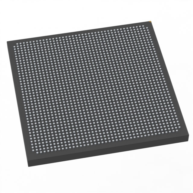
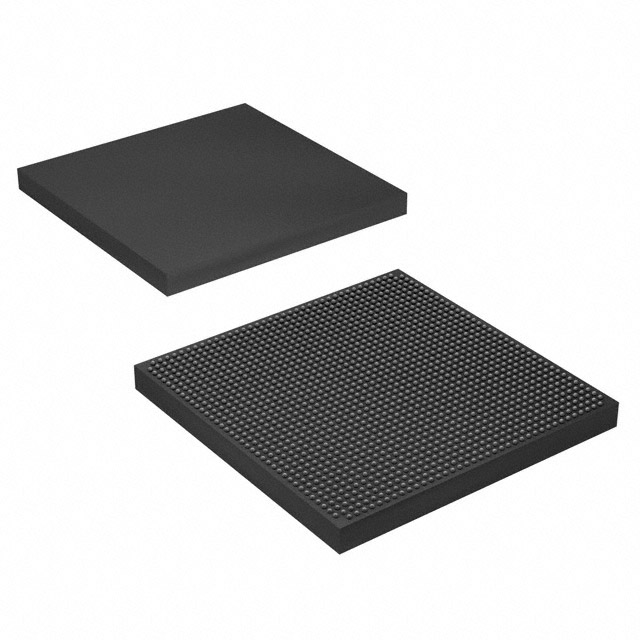
Built in a 1760-ball FCBGA package and specified for extended grade operation, this device targets system designs that require significant logic capacity, embedded memory, and board-level I/O density while operating within a defined core voltage and temperature range.
Key Features
- Logic Capacity — Approximately 1,143,450 logic elements to implement complex custom logic and large-scale designs.
- Configurable Logic Blocks — 65,340 programmable logic blocks (CLBs) to structure logic and routing resources across the device.
- Embedded Memory — Approximately 82.3 Mbits of on-chip RAM for buffering, FIFO, and storage functions within designs.
- I/O Density — 512 I/O pins to support extensive board-level interfacing and multiple peripheral connections.
- Package & Mounting — 1760-BBGA (1760-FCBGA) surface-mount package with supplier package size 42.5 × 42.5 mm for compact board integration.
- Power Supply Range — Core voltage supply specified from 873 mV to 927 mV to match system power rails and sequencing requirements.
- Temperature Grade — Extended grade operating range from 0 °C to 100 °C for deployment in temperature-controlled and general-purpose environments.
- Regulatory Compliance — RoHS compliant.
Typical Applications
- FPGA-based system design — Acts as the central programmable logic device for reconfigurable hardware implementations.
- High-density I/O interfacing — Supports designs that require a large number of external connections with its 512 I/O pins.
- Memory-intensive functions — Uses approximately 82.3 Mbits of embedded memory for buffering, packet storage, or on-chip data handling.
- Custom logic implementation — Leverages roughly 1,143,450 logic elements for implementing extensive custom algorithms and datapaths.
Unique Advantages
- Large logic resource pool: Approximately 1,143,450 logic elements enable implementation of sizeable custom logic and parallel processing blocks.
- Substantial on-chip memory: Around 82.3 Mbits of embedded RAM reduces external memory dependencies for many buffering and storage tasks.
- High I/O count: 512 I/O pins provide flexibility for multi-channel interfaces and dense board connectivity.
- Compact FCBGA package: 1760-ball FCBGA (42.5 × 42.5 mm) supports dense board layouts while maintaining surface-mount assembly.
- Defined power and thermal parameters: Specified core voltage range (873 mV–927 mV) and extended temperature range (0 °C–100 °C) aid system power and thermal planning.
- RoHS compliant: Conforms to RoHS for environmental compliance in many supply chains.
Why Choose XCKU15P-3FFVA1760E?
The XCKU15P-3FFVA1760E combines a very large logic element count, substantial on-chip memory, and a high I/O pin count in a 1760-ball FCBGA package, delivering a balanced platform for FPGA-based system designs that require significant programmable resources. Its specified core voltage range and extended operating temperature make it suitable for general-purpose and temperature-controlled applications.
This device is intended for designers and procurement teams looking for a high-capacity FPGA from AMD with clear, verifiable hardware specifications for logic, memory, I/O, packaging, power, and operating range.
Request a quote or submit an inquiry to begin procurement or to receive pricing and availability information for XCKU15P-3FFVA1760E.


Date Founded: 1969
Headquarters: Santa Clara, California, USA
Employees: 25,000+
Revenue: $22.68 Billion
Certifications and Memberships: ISO9001:2015, RoHS, REACH


