
XCKU15P-L1FFVE1517I
| Part Description |
Kintex® UltraScale+™ Field Programmable Gate Array (FPGA) IC 512 82329600 1143450 1517-BBGA, FCBGA |
|---|---|
| Quantity | 1,604 Available (as of June 18, 2026) |

| Product Category | Field Programmable Gate Array (FPGA) |
|---|---|
| Manufacturer | AMD |
| Manufacturing Status | Active |
| Manufacturer Standard Lead Time | 16 Weeks |
| Datasheet |
Specifications & Environmental
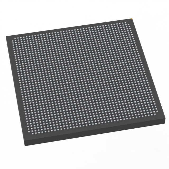
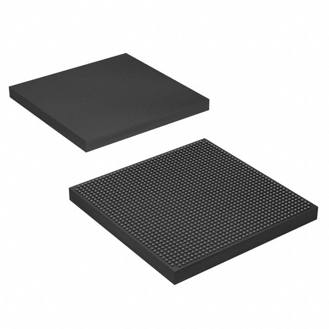
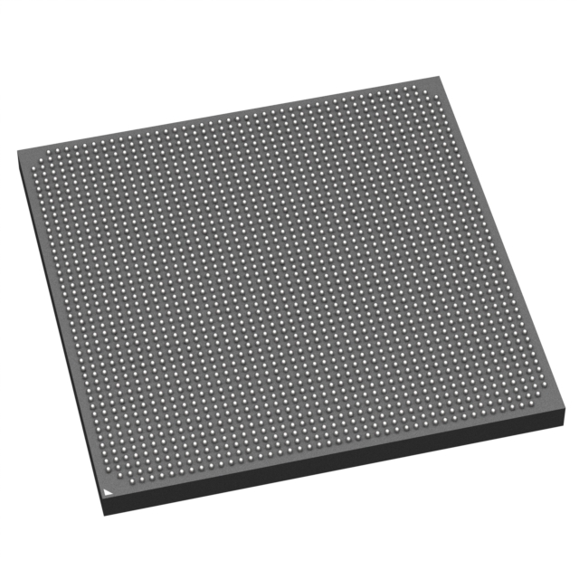
| Device Package | 1517-FCBGA (40x40) | Grade | Industrial | Operating Temperature | -40°C – 100°C | ||
|---|---|---|---|---|---|---|---|
| Package / Case | 1517-BBGA, FCBGA | Number of I/O | 512 | Voltage | 698 mV - 876 mV | ||
| Mounting Method | Surface Mount | RoHS Compliance | ROHS3 Compliant | REACH Compliance | REACH Unknown | ||
| Moisture Sensitivity Level | 4 (72 Hours) | Number of LABs/CLBs | 65340 | Number of Logic Elements/Cells | 1143450 | ||
| Number of Gates | N/A | ECCN | 5A002A1 | HTS Code | 8542.39.0001 | ||
| Qualification | N/A | Total RAM Bits | 82329600 |
Overview of XCKU15P-L1FFVE1517I – Kintex® UltraScale+™ FPGA, 1517-FCBGA (Industrial)
The XCKU15P-L1FFVE1517I is an AMD Kintex® UltraScale+™ field programmable gate array (FPGA) in a 1517-FCBGA package. It provides a high count of programmable logic and embedded memory along with a large I/O complement, packaged for surface-mount assembly and specified for industrial temperature operation.
With approximately 1,143,450 logic elements, roughly 82.33 Mbits of embedded memory and 512 I/O pins, this device is intended for designs that require significant on-chip logic density, embedded RAM capacity, and extensive external connectivity while operating within an industrial temperature range.
Key Features
- Programmable Logic Approximately 1,143,450 logic elements and 65,340 configurable logic blocks (CLBs) provide large-scale programmable resources for complex digital designs.
- Embedded Memory Approximately 82.33 Mbits of on-chip RAM to support buffering, LUT-based storage and memory-intensive functions directly on the FPGA fabric.
- I/O Capacity 512 general-purpose I/O pins enable extensive external interfacing for high-channel-count designs and multiple peripheral connections.
- Package & Mounting 1517-FCBGA (40×40) ball grid array package, surface-mount mounting for compact board-level integration.
- Power Supply Range Core supply specification from 698 mV to 876 mV, allowing clear power budgeting and regulation planning for the FPGA core.
- Operating Temperature Industrial temperature range rated from −40 °C to 100 °C for deployment in harsh or temperature-variable environments.
- Regulatory Compliance RoHS compliant to support lead-free manufacturing processes.
Typical Applications
- High-density digital processing Large logic and CLB counts support complex finite-state machines, custom processors, and heavy combinational logic implementations.
- Memory-intensive functions Approximately 82.33 Mbits of embedded RAM enables on-chip buffering, data aggregation and intermediate storage for streaming and packet-processing tasks.
- Multi-channel I/O systems With 512 I/O pins, the device suits designs requiring broad external connectivity such as multi-channel data acquisition, aggregation, or interface bridging.
- Industrial control and instrumentation Industrial-grade temperature rating and surface-mount packaging make the device appropriate for factory automation, motion control, and industrial communication endpoints that need high logic density.
Unique Advantages
- High on-chip logic capacity: Approximately 1,143,450 logic elements allow consolidation of multiple functions into a single device, reducing board-level part counts.
- Substantial embedded memory: Roughly 82.33 Mbits of RAM reduces dependence on external memory for many buffering and intermediate storage tasks, simplifying system design.
- Extensive I/O connectivity: 512 I/O pins support high channel counts and diverse peripheral interfacing without additional bridging components.
- Industrial temperature support: Rated −40 °C to 100 °C for reliable operation across a wide range of environmental conditions.
- Surface-mount FCBGA package: 1517-FCBGA (40×40) package enables dense PCB layouts and is suitable for automated assembly processes.
- RoHS compliant: Supports lead-free manufacturing flows and regulatory compliance for many global markets.
Why Choose XCKU15P-L1FFVE1517I?
The XCKU15P-L1FFVE1517I positions itself as a high-capacity, industrial-grade FPGA that combines substantial programmable logic, significant embedded RAM and a large I/O complement in a compact FCBGA package. Its electrical and thermal specifications support reliable deployment in designs that demand on-chip resources and robust environmental performance.
This device is well suited for engineers and teams building complex digital systems that benefit from consolidating functionality on a single FPGA—offering scalability for dense logic, memory-backed processing, and extensive external interfacing while aligning with RoHS manufacturing requirements.
Request a quote or submit an inquiry for pricing and availability to get started with XCKU15P-L1FFVE1517I for your next high-density FPGA design.


Date Founded: 1969
Headquarters: Santa Clara, California, USA
Employees: 25,000+
Revenue: $22.68 Billion
Certifications and Memberships: ISO9001:2015, RoHS, REACH


