
XCKU19P-L1FFVJ1760I
| Part Description |
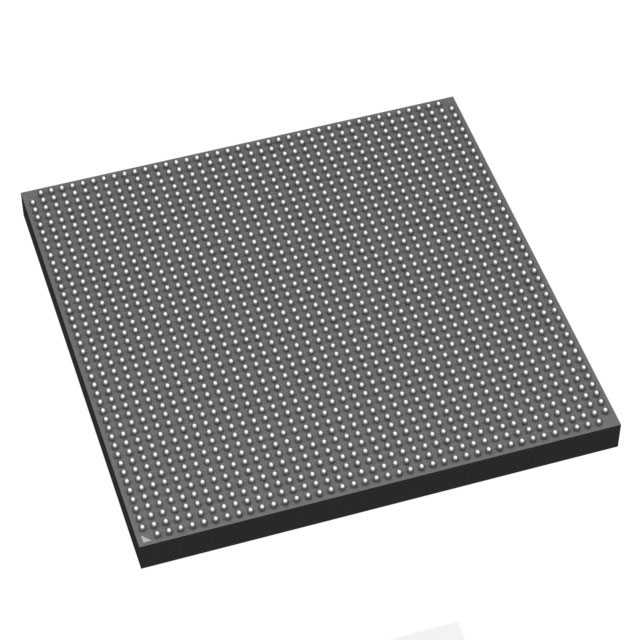
Virtex® UltraScale+™ Field Programmable Gate Array (FPGA) IC 540 63753421 1842750 1760-BBGA, FCBGA |
|---|---|
| Quantity | 622 Available (as of June 15, 2026) |
| Product Category | Field Programmable Gate Array (FPGA) |
|---|---|
| Manufacturer | AMD |
| Manufacturing Status | Active |
| Manufacturer Standard Lead Time | 16 Weeks |
| Datasheet |
Specifications & Environmental
| Device Package | 1760-FCBGA (42.5x42.5) | Grade | Industrial | Operating Temperature | -40°C – 100°C | ||
|---|---|---|---|---|---|---|---|
| Package / Case | 1760-BBGA, FCBGA | Number of I/O | 540 | Voltage | 698 mV - 742 mV | ||
| Mounting Method | Surface Mount | RoHS Compliance | ROHS3 Compliant | REACH Compliance | REACH Unknown | ||
| Moisture Sensitivity Level | 4 (72 Hours) | Number of LABs/CLBs | 105300 | Number of Logic Elements/Cells | 1842750 | ||
| Number of Gates | N/A | ECCN | 3A991D | HTS Code | 8542.39.0001 | ||
| Qualification | N/A | Total RAM Bits | 63753421 |
Overview of XCKU19P-L1FFVJ1760I – Virtex® UltraScale+™ Field Programmable Gate Array, 1760-FCBGA (42.5 × 42.5), Industrial
The XCKU19P-L1FFVJ1760I is a high-density Virtex® UltraScale+™ FPGA IC from AMD, supplied in a 1760-FCBGA package. It combines a very large pool of programmable logic, substantial embedded memory, and a high I/O count in a surface-mount FCBGA footprint designed for industrial-class environments.
Engineered for designs that require extensive on-chip resources and robust operating conditions, this device targets applications demanding high logic capacity, significant embedded RAM, and broad peripheral connectivity while meeting industrial temperature requirements.
Key Features
- High Logic Density — 1,842,750 logic elements to implement large-scale digital designs and complex custom logic functions.
- Embedded Memory — approximately 64 Mbits of on-chip RAM (63,753,421 bits) to support buffering, state storage, and data processing tasks without external memory.
- Extensive I/O — 540 I/O pins for broad peripheral interfacing, multi-channel connectivity, and system integration.
- Power Supply Range — operates with a core voltage supply range of 698 mV to 742 mV as specified for device power planning.
- Industrial Temperature Range — rated for operation from −40 °C to 100 °C for deployment in industrial environments.
- Package & Mounting — supplied in a 1760-FCBGA package (42.5 × 42.5 mm) with surface-mount mounting for dense PCB integration.
- Compliance — RoHS compliant to support regulatory and environmental requirements.
Typical Applications
- High-density digital processing — implement large, custom datapaths and control logic using the device’s 1,842,750 logic elements and substantial on-chip RAM.
- Multi-channel I/O systems — systems requiring many parallel interfaces can take advantage of the 540 available I/O pins for sensors, transceivers, or peripheral buses.
- Industrial embedded systems — suitable for industrial deployments that need a surface-mount FPGA with an operating range from −40 °C to 100 °C.
Unique Advantages
- Massive programmable capacity: 1,842,750 logic elements enable consolidation of complex functions into a single FPGA, reducing system-level component count.
- Significant on-chip memory: approximately 64 Mbits of embedded RAM reduces dependence on external memory and improves data throughput and latency.
- Broad connectivity: 540 I/O pins provide flexibility to interface with numerous peripherals and high-channel-count systems without external multiplexing.
- Industrial readiness: rated for −40 °C to 100 °C operation for reliable use in demanding environments.
- Compact board-level integration: 1760-FCBGA (42.5 × 42.5 mm) surface-mount package supports high-density PCB designs.
- Regulatory compliance: RoHS compliant for environmentally conscious product development.
Why Choose XCKU19P-L1FFVJ1760I?
The XCKU19P-L1FFVJ1760I combines very high logic element capacity, substantial embedded memory, and an extensive I/O complement in a rugged industrial-rated FPGA package. It is suited to designs that require consolidation of complex digital functions, significant on-chip buffering, and numerous external interfaces while meeting industrial temperature requirements.
For engineering teams focused on high-capacity, scalable FPGA implementations, this device offers the on-chip resources and form factor necessary to reduce system complexity and support long-term design objectives in industrial applications.
Request a quote or submit an inquiry for pricing and availability to move your design forward with the XCKU19P-L1FFVJ1760I.


Date Founded: 1969
Headquarters: Santa Clara, California, USA
Employees: 25,000+
Revenue: $22.68 Billion
Certifications and Memberships: ISO9001:2015, RoHS, REACH


