
XCKU3P-1FFVD900E
| Part Description |
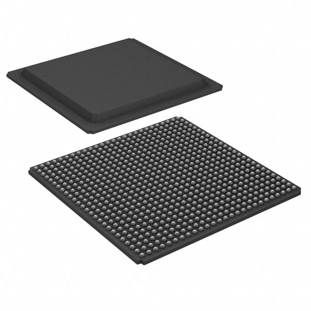
Kintex® UltraScale+™ Field Programmable Gate Array (FPGA) IC 304 31641600 355950 900-BBGA, FCBGA |
|---|---|
| Quantity | 470 Available (as of June 15, 2026) |

| Product Category | Field Programmable Gate Array (FPGA) |
|---|---|
| Manufacturer | AMD |
| Manufacturing Status | Active |
| Manufacturer Standard Lead Time | 16 Weeks |
| Datasheet |
Specifications & Environmental
| Device Package | 900-FCBGA (31x31) | Grade | Extended | Operating Temperature | 0°C – 100°C | ||
|---|---|---|---|---|---|---|---|
| Package / Case | 900-BBGA, FCBGA | Number of I/O | 304 | Voltage | 825 mV - 876 mV | ||
| Mounting Method | Surface Mount | RoHS Compliance | ROHS3 Compliant | REACH Compliance | REACH Unaffected | ||
| Moisture Sensitivity Level | 4 (72 Hours) | Number of LABs/CLBs | 20340 | Number of Logic Elements/Cells | 355950 | ||
| Number of Gates | N/A | ECCN | 3A991D | HTS Code | 8542.39.0001 | ||
| Qualification | N/A | Total RAM Bits | 31641600 |
Overview of XCKU3P-1FFVD900E – Kintex® UltraScale+™ FPGA, 355,950 logic elements, 304 I/O (900-FCBGA)
The XCKU3P-1FFVD900E is a Kintex® UltraScale+™ Field Programmable Gate Array (FPGA) provided in a 900-ball FCBGA package. It delivers a high-density programmable logic fabric paired with substantial on-chip memory and a broad I/O complement for demanding digital designs.
Designed for applications that require significant logic resources and embedded memory, this device combines 355,950 logic elements, approximately 31.6 Mbits of embedded memory, and 304 I/O pins in a surface-mount 900-FCBGA (31×31) package. The device operates over a core voltage range of 825 mV to 876 mV and an operating temperature range of 0°C to 100°C.
Key Features
- Core Architecture Kintex® UltraScale+™ Field Programmable Gate Array family—programmable logic fabric for custom digital implementations.
- Logic Capacity Approximately 355,950 logic elements enabling implementation of complex logic, control, and datapath structures.
- Embedded Memory Approximately 31.6 Mbits of on-chip RAM for buffering, FIFOs, and local storage.
- I/O and Package 304 user I/O pins in a 900-FCBGA surface-mount package; supplier device package specified as 900-FCBGA (31×31).
- Power Core voltage supply range of 825 mV to 876 mV for the FPGA core domain.
- Thermal and Grade Extended grade device with an operating temperature range of 0°C to 100°C.
- Compliance and Mounting RoHS compliant and supplied in a surface-mount FCBGA package.
Typical Applications
- High-density digital processing Implement complex logic and datapath operations using the large logic element count and embedded memory.
- Multi-channel I/O systems Leverage 304 I/O pins for interfacing multiple peripherals, sensors, or high-channel-count front ends.
- On-chip buffering and storage Use approximately 31.6 Mbits of embedded RAM for local buffering, packet queues, or temporary storage.
- Platform prototypes and custom hardware Utilize the programmable fabric and substantial resources for prototyping system-level FPGA designs.
Unique Advantages
- High logic density: Approximately 355,950 logic elements provide room for large-scale integration of custom logic blocks and state machines.
- Significant embedded memory: Roughly 31.6 Mbits of on-chip RAM reduces reliance on external memory for local buffering and accelerates data handling.
- Broad I/O capacity: 304 I/O pins support multi-channel interfacing and flexible board-level connectivity options.
- Compact surface-mount packaging: 900-FCBGA (31×31) package offers a dense solution for space-constrained board layouts.
- Controlled core power range: A defined core voltage supply range (825 mV to 876 mV) aids in power domain planning and regulator selection.
- RoHS compliant: Environmentally compliant manufacturing and end-of-life handling.
Why Choose XCKU3P-1FFVD900E?
The XCKU3P-1FFVD900E positions itself as a high-capacity, feature-rich FPGA option for designs that demand large logic resources, substantial on-chip memory, and extensive I/O in a compact surface-mount package. Its extended-grade rating and defined operating range provide predictable behavior across typical commercial temperature conditions.
This device is well suited to engineering teams building complex programmable systems that require integration of many logic functions and local memory without immediately resorting to large external memory subsystems. The combination of logic density, on-chip RAM, and 304 I/O delivers a scalable platform for advanced digital designs while maintaining RoHS compliance.
Request a quote or submit an inquiry to obtain pricing, availability, or additional technical information for the XCKU3P-1FFVD900E.


Date Founded: 1969
Headquarters: Santa Clara, California, USA
Employees: 25,000+
Revenue: $22.68 Billion
Certifications and Memberships: ISO9001:2015, RoHS, REACH


