
XCKU3P-2FFVD900E
| Part Description |
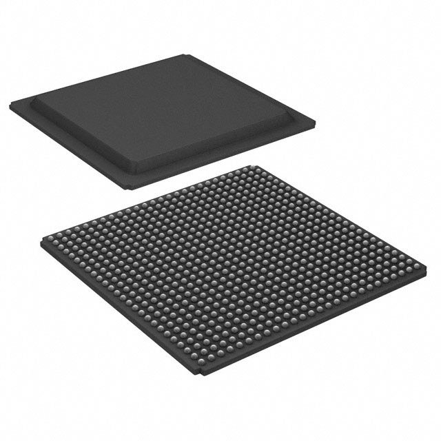
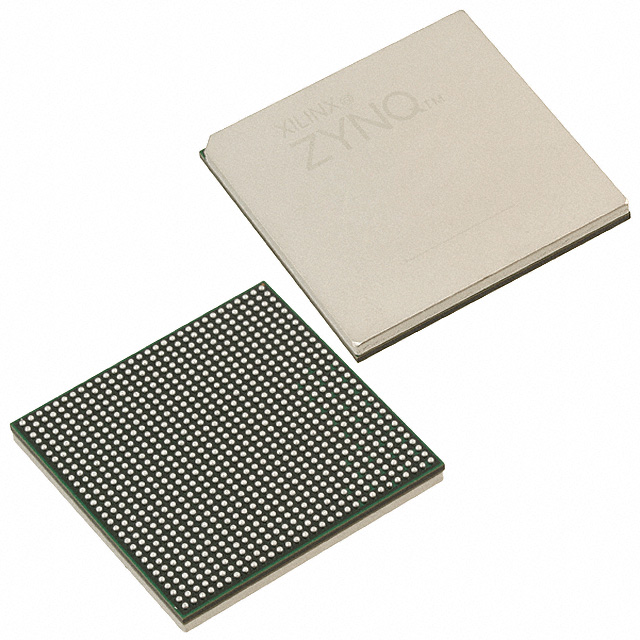
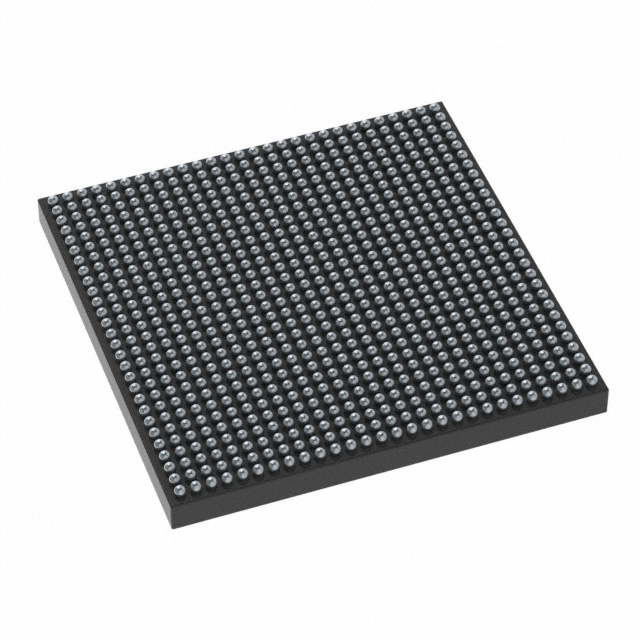
Kintex® UltraScale+™ Field Programmable Gate Array (FPGA) IC 304 31641600 355950 900-BBGA, FCBGA |
|---|---|
| Quantity | 1,011 Available (as of June 14, 2026) |

| Product Category | Field Programmable Gate Array (FPGA) |
|---|---|
| Manufacturer | AMD |
| Manufacturing Status | Active |
| Manufacturer Standard Lead Time | 16 Weeks |
| Datasheet |
Specifications & Environmental
| Device Package | 900-FCBGA (31x31) | Grade | Extended | Operating Temperature | 0°C – 100°C | ||
|---|---|---|---|---|---|---|---|
| Package / Case | 900-BBGA, FCBGA | Number of I/O | 304 | Voltage | 825 mV - 876 mV | ||
| Mounting Method | Surface Mount | RoHS Compliance | ROHS3 Compliant | REACH Compliance | REACH Unknown | ||
| Moisture Sensitivity Level | 4 (72 Hours) | Number of LABs/CLBs | 20340 | Number of Logic Elements/Cells | 355950 | ||
| Number of Gates | N/A | ECCN | 3A991D | HTS Code | 8542.39.0001 | ||
| Qualification | N/A | Total RAM Bits | 31641600 |
Overview of XCKU3P-2FFVD900E – Kintex® UltraScale+ Field Programmable Gate Array, 900‑BBGA, 304 I/O
The XCKU3P-2FFVD900E is a Kintex® UltraScale+™ field programmable gate array (FPGA) IC from AMD supplied in a 900‑ball FCBGA package. It delivers high logic density, substantial on-chip memory, and a large I/O count for designs that require programmable hardware resources in a compact surface‑mount form factor.
With approximately 355,950 logic elements, about 31.6 Mbits of embedded memory and up to 304 I/O, this device targets applications that need extensive programmable logic, embedded storage, and reliable I/O connectivity while operating within a defined supply and temperature window.
Key Features
- Core Logic Contains approximately 355,950 logic elements and 20,340 CLBs for implementing large, complex programmable logic designs.
- Embedded Memory Provides approximately 31.6 Mbits of on‑chip RAM for buffering, data staging and local storage of intermediate results.
- I/O Capacity Up to 304 general‑purpose I/O pins support substantial peripheral and system interfacing in a single device.
- Power Supply Core voltage supply range is specified between 825 mV and 876 mV, enabling operation within the device’s defined low‑voltage core range.
- Package & Mounting Supplied in a 900‑BBGA FCBGA package (900‑FCBGA, 31×31) optimized for surface‑mount PCB assembly and high‑density board layouts.
- Operating Range & Grade Extended grade device with an operating temperature range of 0 °C to 100 °C for applications within that thermal envelope.
- Environmental Compliance RoHS compliant construction supports regulatory requirements for lead‑free assembly.
Typical Applications
- Compute Acceleration Implement custom data‑path logic and hardware accelerators using the device’s large logic element count and on‑chip memory.
- High‑Density I/O and Protocol Bridging Leverage 304 I/O in the 900‑ball FCBGA package to consolidate multiple interfaces and perform protocol conversion in a compact footprint.
- System Prototyping and Integration Use reprogrammable logic and embedded RAM to validate system architectures and integrate complex functions on a single chip.
Unique Advantages
- High Logic Density: Approximately 355,950 logic elements enable integration of complex, multi‑block designs without partitioning across multiple devices.
- Substantial On‑Chip Memory: About 31.6 Mbits of embedded RAM reduce dependence on external memory for many buffering and staging tasks.
- Large I/O Count in a Compact Package: 304 I/O in a 900‑FCBGA (31×31) footprint supports rich external connectivity while maintaining a small PCB area.
- Defined Low‑Voltage Core Supply: Core operation between 825 mV and 876 mV supports designs targeting modern low‑voltage logic domains.
- Extended Grade and RoHS Compliance: Extended grade temperature rating and RoHS compliance provide clear environmental and thermal characteristics for deployment planning.
Why Choose XCKU3P-2FFVD900E?
The XCKU3P-2FFVD900E positions itself as a high‑density, highly configurable FPGA solution for engineers who need significant programmable logic, embedded memory and a large number of I/O in a single surface‑mount package. Its combination of approximately 355,950 logic elements, roughly 31.6 Mbits of RAM and 304 I/O pins makes it suitable for consolidating complex functions and accelerating custom processing workloads.
Backed by AMD as the manufacturer and supported by UltraScale+ family documentation, this device is appropriate for teams seeking scalable FPGA resources with defined electrical, thermal and packaging characteristics to plan board‑level integration and procurement.
Request a quote or submit an inquiry to obtain pricing, lead time and availability for the XCKU3P-2FFVD900E. Provide your quantity and requirements to receive a tailored response.


Date Founded: 1969
Headquarters: Santa Clara, California, USA
Employees: 25,000+
Revenue: $22.68 Billion
Certifications and Memberships: ISO9001:2015, RoHS, REACH


