
XCKU5P-1SFVB784E
| Part Description |
Kintex® UltraScale+™ Field Programmable Gate Array (FPGA) IC 304 41984000 474600 784-BFBGA, FCBGA |
|---|---|
| Quantity | 1,349 Available (as of June 15, 2026) |
| Product Category | Field Programmable Gate Array (FPGA) |
|---|---|
| Manufacturer | AMD |
| Manufacturing Status | Active |
| Manufacturer Standard Lead Time | 16 Weeks |
| Datasheet |
Specifications & Environmental
| Device Package | 784-FCBGA (23x23) | Grade | Extended | Operating Temperature | 0°C – 100°C | ||
|---|---|---|---|---|---|---|---|
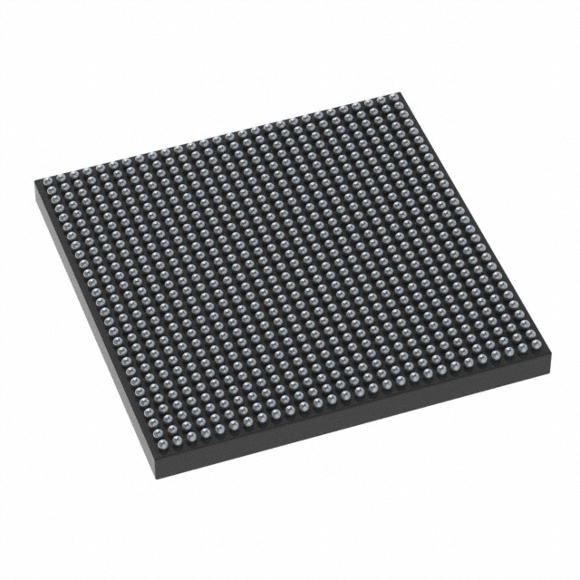
| Package / Case | 784-BFBGA, FCBGA | Number of I/O | 304 | Voltage | 825 mV - 876 mV | ||
| Mounting Method | Surface Mount | RoHS Compliance | ROHS3 Compliant | REACH Compliance | REACH Unknown | ||
| Moisture Sensitivity Level | 4 (72 Hours) | Number of LABs/CLBs | 27120 | Number of Logic Elements/Cells | 474600 | ||
| Number of Gates | N/A | ECCN | 3A991D | HTS Code | 8542.39.0001 | ||
| Qualification | N/A | Total RAM Bits | 41984000 |
Overview of XCKU5P-1SFVB784E – Kintex® UltraScale+™ FPGA IC, 304 I/O, 784-FCBGA
The XCKU5P-1SFVB784E is an AMD Kintex® UltraScale+™ Field Programmable Gate Array supplied in a 784-BFBGA (784-FCBGA, 23×23) surface-mount package. It provides a high logic-capacity FPGA fabric with substantial embedded RAM and a large I/O count for complex, resource‑intensive designs.
Key on-chip resources include 474,600 logic elements, approximately 42 Mbits of embedded memory (41,984,000 bits), and 304 general-purpose I/O pins. The device is an extended-grade part with a specified operating temperature range of 0 °C to 100 °C and a core voltage supply range of 825 mV to 876 mV.
Key Features
- Core Logic 474,600 logic elements provide ample capacity for large-scale digital designs and custom logic implementations.
- Configurable Logic Blocks (CLBs) 27,120 CLBs for structured logic partitioning and resource planning.
- Embedded Memory Approximately 42 Mbits of on-chip RAM (41,984,000 bits) to support buffering, FIFOs, and memory‑intensive functions.
- I/O Resources 304 I/O pins support multi-channel interfacing and high pin-count connectivity in a single device.
- Power and Voltage Specified core voltage supply range from 825 mV to 876 mV for predictable power planning and board design.
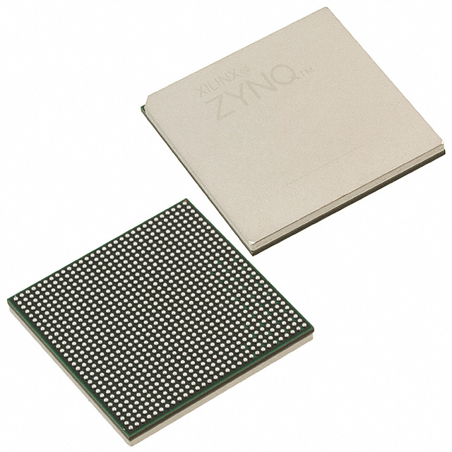
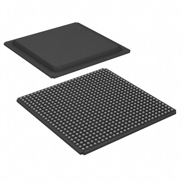
- Package and Mounting 784-BFBGA (supplier package: 784-FCBGA, 23×23) in a surface-mount package suitable for compact PCB integration.
- Operating Conditions Extended-grade device with an operating temperature range of 0 °C to 100 °C.
- Compliance RoHS compliant.
Typical Applications
- FPGA-based compute acceleration Use the large logic element count and embedded memory to implement hardware-accelerated algorithms and custom datapaths.
- High‑I/O aggregation 304 I/O pins enable designs that consolidate multiple interfaces or high-channel-count front-ends on a single FPGA.
- Memory-centric buffering and processing Approximately 42 Mbits of on-chip RAM supports data buffering, streaming, and intermediate storage within complex pipelines.
Unique Advantages
- High logic capacity: 474,600 logic elements allow implementation of large and complex logic designs without immediate partitioning across multiple devices.
- Ample embedded memory: Approximately 42 Mbits of on-chip RAM reduces dependence on external memory for many buffering and intermediate storage needs.
- Generous I/O count: 304 I/O pins simplify integration of multiple interfaces and high-channel-count systems on a single FPGA.
- Compact BGA package: 784-FCBGA (23×23) package provides a high-density solution for space‑constrained PCBs while maintaining extensive device resources.
- Controlled supply range: Narrow voltage supply window (825 mV–876 mV) supports consistent power planning and predictable core behavior.
- Extended-grade operation: Rated for 0 °C to 100 °C operating range to meet a range of commercial and extended-environment applications.
Why Choose XCKU5P-1SFVB784E?
The XCKU5P-1SFVB784E combines substantial logic resources, significant embedded memory, and a high I/O count in a compact 784-FCBGA surface-mount package. Its extended-grade rating and defined core voltage window make it a suitable option for engineering teams designing complex systems that require integrated logic capacity and on-chip storage.
This device is well suited to designers seeking a single‑chip solution for dense logic implementations, high-channel interfacing, and memory‑heavy processing, offering predictable electrical and thermal parameters for board-level integration and system planning.
Request a quote or contact sales to discuss availability, pricing, and how the XCKU5P-1SFVB784E can fit into your next design.


Date Founded: 1969
Headquarters: Santa Clara, California, USA
Employees: 25,000+
Revenue: $22.68 Billion
Certifications and Memberships: ISO9001:2015, RoHS, REACH


