
XCKU5P-2SFVB784E
| Part Description |
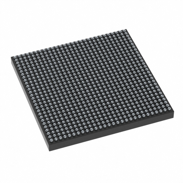
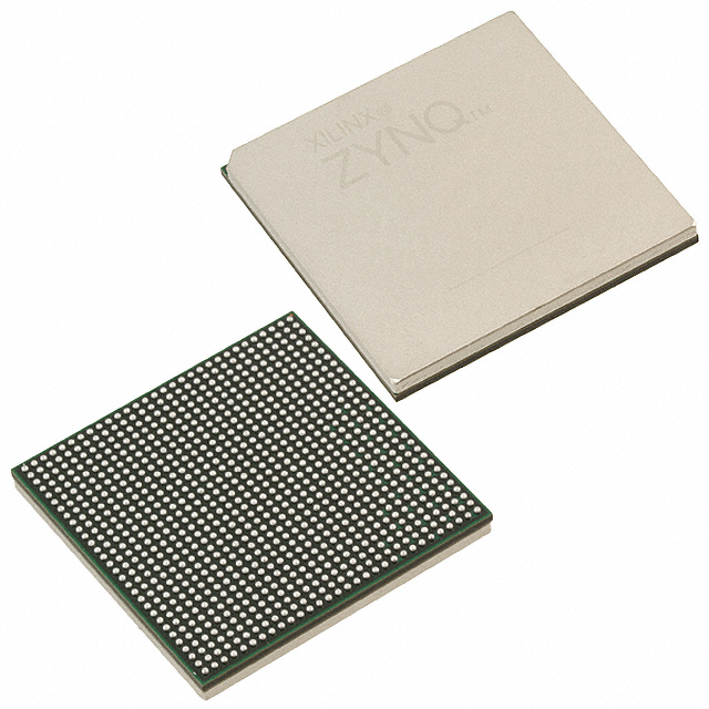
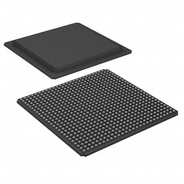
Kintex® UltraScale+™ Field Programmable Gate Array (FPGA) IC 304 41984000 474600 784-BFBGA, FCBGA |
|---|---|
| Quantity | 1,428 Available (as of June 15, 2026) |

| Product Category | Field Programmable Gate Array (FPGA) |
|---|---|
| Manufacturer | AMD |
| Manufacturing Status | Active |
| Manufacturer Standard Lead Time | 16 Weeks |
| Datasheet |
Specifications & Environmental
| Device Package | 784-FCBGA (23x23) | Grade | Extended | Operating Temperature | 0°C – 100°C | ||
|---|---|---|---|---|---|---|---|
| Package / Case | 784-BFBGA, FCBGA | Number of I/O | 304 | Voltage | 825 mV - 876 mV | ||
| Mounting Method | Surface Mount | RoHS Compliance | ROHS3 Compliant | REACH Compliance | REACH Unknown | ||
| Moisture Sensitivity Level | 4 (72 Hours) | Number of LABs/CLBs | 27120 | Number of Logic Elements/Cells | 474600 | ||
| Number of Gates | N/A | ECCN | 3A991D | HTS Code | 8542.39.0001 | ||
| Qualification | N/A | Total RAM Bits | 41984000 |
Overview of XCKU5P-2SFVB784E – Kintex® UltraScale+™ Field Programmable Gate Array (FPGA), 784‑FCBGA (23×23), 304 I/O
The XCKU5P-2SFVB784E is a Kintex® UltraScale+™ FPGA IC that delivers a substantial logic and memory footprint in a 784-ball FCBGA package. It combines a large number of logic elements, on-chip RAM, and a high I/O count to support complex, custom digital designs.
Key device attributes include 474,600 logic elements, approximately 42 Mbits of embedded memory, 304 I/O, an extended grade operating range of 0 °C to 100 °C, and a supply range of 825 mV to 876 mV — enabling compact, high-density implementations where these electrical and thermal conditions match design requirements.
Key Features
- Core Logic Capacity 474,600 logic elements provide a large fabric for implementing custom digital logic, algorithms, and glue logic within a single device.
- Embedded Memory Approximately 42 Mbits of on-chip RAM support buffering, state storage, and local data processing without external memory for many use cases.
- I/O Density 304 general-purpose I/O pins enable broad interfacing to peripherals, sensors, and external subsystems.
- Power Supply Range Operates with a core supply range of 825 mV to 876 mV, allowing designs to target the specified voltage envelope.
- Package & Mounting Supplied in a 784‑FCBGA package (23×23) for surface-mount PCB assembly, providing a compact footprint for high-density boards.
- Operating Grade & Temperature Extended grade with an operating temperature range of 0 °C to 100 °C to meet applications requiring elevated-temperature operation within that window.
- Environmental Compliance RoHS compliant, meeting common regulatory requirements for lead-free assembly.
Typical Applications
- Custom Digital Processing — Use the device's 474,600 logic elements and embedded memory to implement bespoke datapaths, accelerators, and control logic tailored to specific system requirements.
- Memory-Intensive Functions — Approximately 42 Mbits of on-chip RAM supports local buffering, queueing, and state machines without immediate reliance on external memory.
- High‑Pin-Count Interfaces — The 304 I/O pins facilitate integration with multiple peripherals, sensors, and I/O boards where numerous signals are required.
- Compact System Integration — The 784‑FCBGA (23×23) surface-mount package enables dense PCB layouts for space-constrained designs that require substantial logic and I/O.
Unique Advantages
- Large Logic Resource: 474,600 logic elements allow extensive on-chip implementation of complex logic, reducing the need for multiple devices.
- Significant Embedded Memory: Approximately 42 Mbits of RAM supports local data handling and reduces dependency on external memory subsystems.
- Extensive I/O: 304 I/O pins provide flexibility for interfacing with a wide range of external components and systems.
- Compact FCBGA Package: The 784‑ball FCBGA (23×23) offers a high-density form factor suitable for tightly-packed board designs.
- Extended Operating Range: Rated for 0 °C to 100 °C operation, matching applications that require above-typical commercial temperature tolerance within that range.
- RoHS Compliant: Meets lead-free assembly requirements for environmentally conscious production.
Why Choose XCKU5P-2SFVB784E?
The XCKU5P-2SFVB784E positions itself as a high-capacity, on-chip resource for designs that need substantial logic, embedded memory, and broad I/O in a compact FCBGA package. Its combination of 474,600 logic elements, approximately 42 Mbits of embedded RAM, and 304 I/O pins makes it well suited to consolidate complex functions into a single programmable device while operating within a defined 825 mV–876 mV supply range and 0 °C–100 °C temperature window.
This device is appropriate for engineering teams and procurement seeking a programmable IC with large on-chip resources, a dense package footprint (784‑FCBGA, 23×23), and extended-grade operating specifications for applications aligned with the stated electrical and thermal limits.
Request a quote or submit an inquiry to receive pricing and availability information for the XCKU5P-2SFVB784E.


Date Founded: 1969
Headquarters: Santa Clara, California, USA
Employees: 25,000+
Revenue: $22.68 Billion
Certifications and Memberships: ISO9001:2015, RoHS, REACH


