
XCKU5P-3FFVB676E
| Part Description |
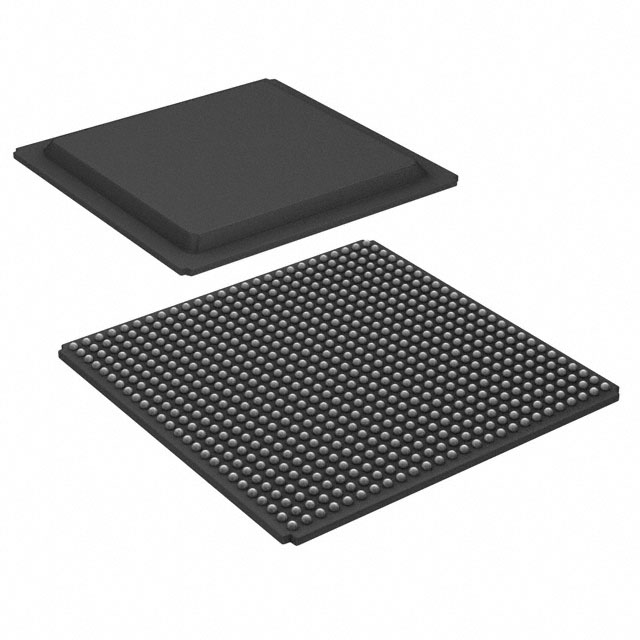
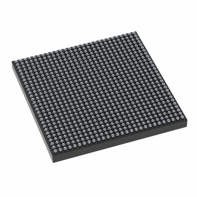
Kintex® UltraScale+™ Field Programmable Gate Array (FPGA) IC 280 41984000 474600 676-BBGA, FCBGA |
|---|---|
| Quantity | 1,091 Available (as of October 8, 2026) |
| Product Category | Field Programmable Gate Array (FPGA) |
|---|---|
| Manufacturer | AMD |
| Manufacturing Status | Active |
| Manufacturer Standard Lead Time | 16 Weeks |
| Datasheet |
Specifications & Environmental
| Device Package | 676-FCBGA (27x27) | Grade | Extended | Operating Temperature | 0°C – 100°C | ||
|---|---|---|---|---|---|---|---|
| Package / Case | 676-BBGA, FCBGA | Number of I/O | 280 | Voltage | 825 mV - 876 mV | ||
| Mounting Method | Surface Mount | RoHS Compliance | ROHS3 Compliant | REACH Compliance | REACH Unaffected | ||
| Moisture Sensitivity Level | 4 (72 Hours) | Number of LABs/CLBs | 27120 | Number of Logic Elements/Cells | 474600 | ||
| Number of Gates | N/A | ECCN | 3A001A7B | HTS Code | 8542.39.0001 | ||
| Qualification | N/A | Total RAM Bits | 41984000 |
Overview of XCKU5P-3FFVB676E – Kintex® UltraScale+™ Field Programmable Gate Array (FPGA), 676-FCBGA
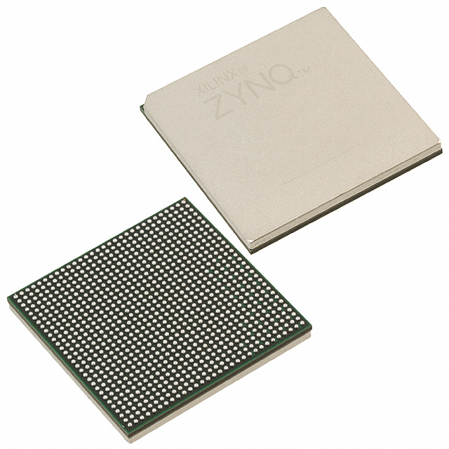
The XCKU5P-3FFVB676E is a Kintex® UltraScale+™ Field Programmable Gate Array (FPGA) offered in a 676-FCBGA package. It provides a high-density programmable fabric with extensive on-chip memory and a large I/O count for designs that require significant logic capacity and interface density.
This extended-grade device is suited to applications where high logic element count, substantial embedded RAM, and a compact surface-mount package are primary design drivers. The device operates within a specified core voltage range and an ambient operating temperature range for reliable system integration.
Key Features
- Core Logic Capacity Provides 474,600 logic elements to implement complex digital designs and large-scale programmable logic functions.
- Embedded Memory Includes approximately 42 Mbits of on-chip RAM (41,984,000 bits) for data buffering, FIFOs, and local storage within the FPGA fabric.
- I/O Count Offers 280 user I/Os to support multi-channel interfacing and dense board-level connectivity.
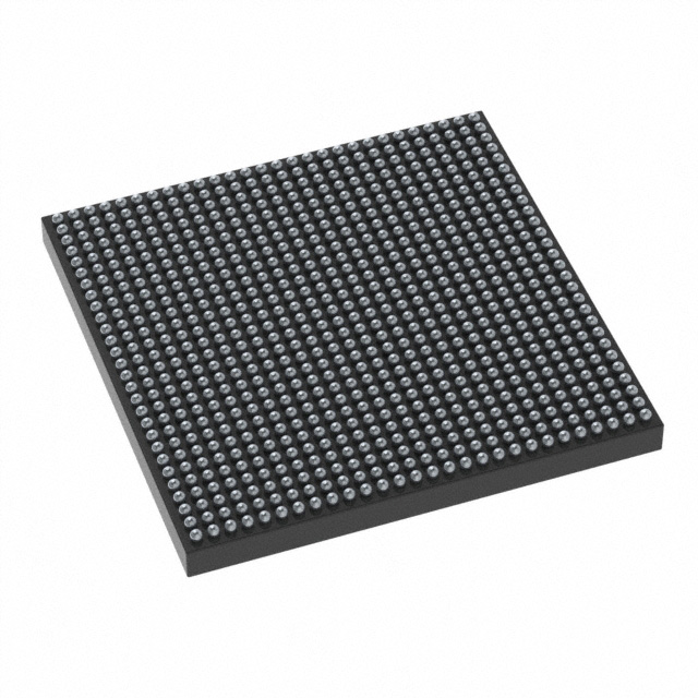
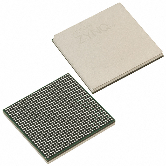
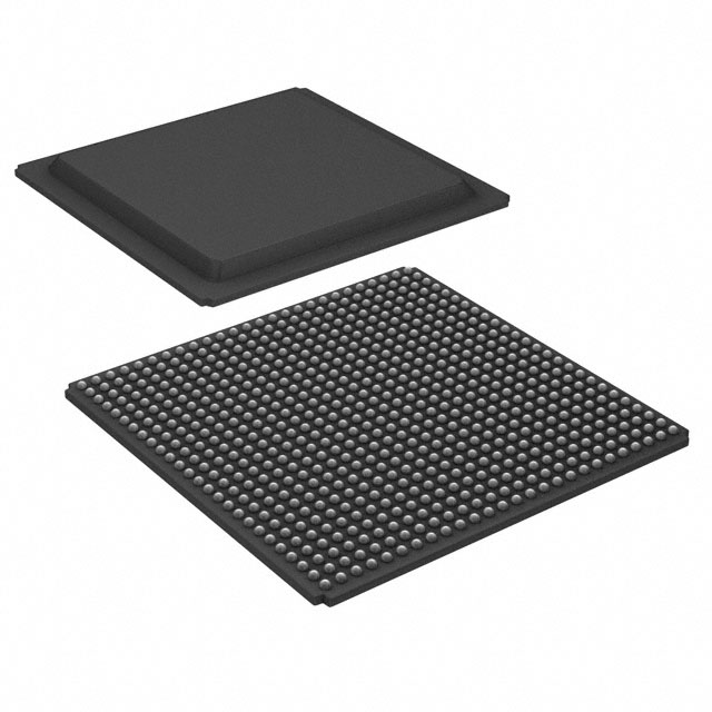
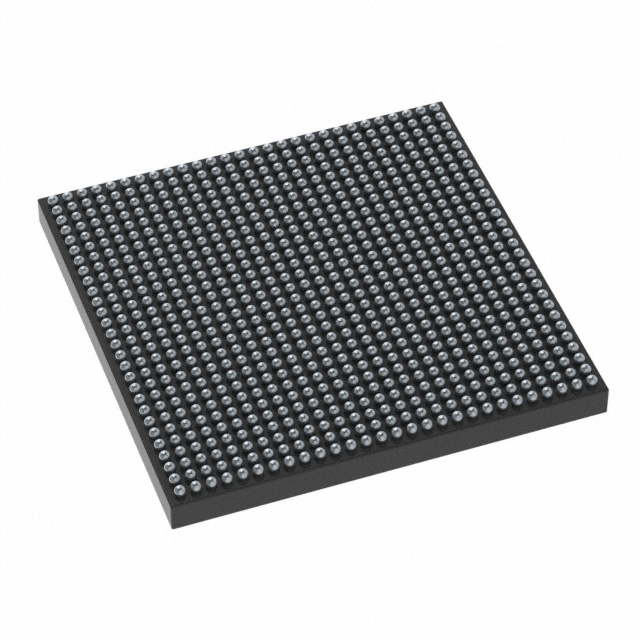
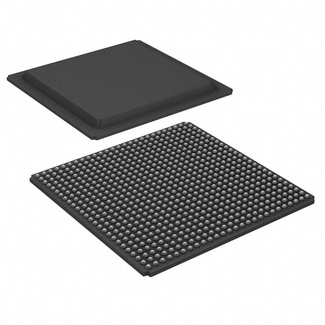
- Package and Mounting Delivered in a 676-BBGA, FCBGA package with supplier device package listed as 676-FCBGA (27×27), designed for surface-mount assembly.
- Power Core supply operating range specified from 825 mV to 876 mV to match system power budgeting and regulator selection.
- Operating Range and Grade Extended grade device with an operating temperature range of 0 °C to 100 °C for a broad set of commercial and extended-environment applications.
- Regulatory RoHS compliant, aiding compliance with common environmental requirements.
Typical Applications
- High-density digital processing Leverages the large logic element count and on-chip RAM for implementing complex signal processing, protocol handling, and control logic.
- Multi-I/O interface hubs Uses the 280 I/Os to consolidate and bridge multiple peripheral or board-level interfaces in compact systems.
- Prototyping and system integration Provides a high-capacity programmable platform for hardware validation and integration tasks where on-chip resources reduce external component count.
Unique Advantages
- High logic density: 474,600 logic elements enable implementation of large, feature-rich designs without offloading core functions to external devices.
- Substantial embedded memory: Approximately 42 Mbits of on-chip RAM reduce dependence on external memory for buffering and temporary storage, simplifying PCB design.
- Extensive I/O capability: 280 available I/Os support multi-channel connectivity and flexible board-level interfacing options.
- Compact, surface-mount package: 676-FCBGA (27×27) offers a high-density package footprint suitable for space-constrained designs while maintaining robust mounting.
- Controlled supply range: Defined core voltage range (825 mV–876 mV) aids predictable power design and regulator selection.
- Extended-grade operation: Rated for 0 °C–100 °C operation to meet a range of commercial and extended-environment deployment scenarios.
Why Choose XCKU5P-3FFVB676E?
The XCKU5P-3FFVB676E positions itself as a high-capacity Kintex® UltraScale+™ FPGA option for engineers who require abundant logic resources, significant embedded memory, and a large number of I/Os in a compact surface-mount FCBGA package. Its defined core voltage range and extended operating temperature make it suitable for designs demanding predictable electrical and thermal behavior.
This device is appropriate for teams developing complex digital systems, multi-interface controllers, and prototype platforms where on-chip resources can reduce external BOM and simplify system integration. Being part of the Kintex UltraScale+ family provides a clear pathway for leveraging series-level capabilities in scalable designs.
Request a quote or submit an inquiry to receive pricing, availability, and ordering information for the XCKU5P-3FFVB676E.





















Date Founded: 1969
Headquarters: Santa Clara, California, USA
Employees: 25,000+
Revenue: $22.68 Billion
Certifications and Memberships: ISO9001:2015, RoHS, REACH











