
XCV200E-6FG256I
| Part Description |
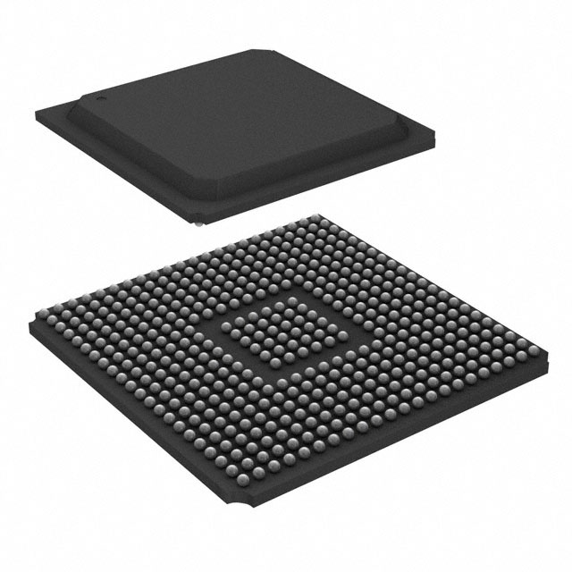
Virtex®-E Field Programmable Gate Array (FPGA) IC 176 114688 5292 256-BGA |
|---|---|
| Quantity | 1,064 Available (as of June 15, 2026) |

| Product Category | Field Programmable Gate Array (FPGA) |
|---|---|
| Manufacturer | AMD |
| Manufacturing Status | Obsolete |
| Manufacturer Standard Lead Time | Contact Us |
| Datasheet |
Specifications & Environmental
| Device Package | 256-FBGA (17x17) | Grade | Industrial | Operating Temperature | -40°C – 100°C | ||
|---|---|---|---|---|---|---|---|
| Package / Case | 256-BGA | Number of I/O | 176 | Voltage | 1.71 V - 1.89 V | ||
| Mounting Method | Surface Mount | RoHS Compliance | RoHS non-compliant | REACH Compliance | REACH Unaffected | ||
| Moisture Sensitivity Level | 3 (168 Hours) | Number of LABs/CLBs | 1176 | Number of Logic Elements/Cells | 5292 | ||
| Number of Gates | 306393 | ECCN | 3A001A7B | HTS Code | 8542.39.0001 | ||
| Qualification | N/A | Total RAM Bits | 114688 |
Overview of XCV200E-6FG256I – Virtex®-E FPGA, 256‑BGA, Industrial Grade
The XCV200E-6FG256I is a Virtex®-E family field programmable gate array (FPGA) in a 256‑FBGA (17×17) package, designed for industrial-grade, reconfigurable logic applications. This 1.8 V-class FPGA provides 5,292 logic elements, approximately 114,688 bits of on-chip RAM and 176 user I/O pins, addressing mid-range integration needs where in-system programmability and robust I/O are required.
With an operating temperature range from −40 °C to 100 °C and RoHS compliance, the device targets industrial applications that require wide temperature operation, significant I/O density and flexible memory structures.
Key Features
- Logic Capacity and Fabric 5,292 logic elements and approximately 306,393 system gates provide a reconfigurable fabric for custom logic, control, and glue‑logic implementations.
- Embedded Memory Approximately 114,688 bits of on-chip RAM for distributed and block memory usage, supporting data buffering and local storage.
- I/O and Interface Flexibility 176 I/O pins with SelectI/O+ style capabilities described in the Virtex‑E family documentation, offering support for multiple high-performance interface standards and differential signalling (LVDS, BLVDS, LVPECL).
- Performance and Clocking Family-level timing includes internal performance up to 130 MHz (four LUT levels) and sophisticated clock management with multiple DLLs for clock multiply/divide and duty‑cycle control, aiding high-speed synchronous designs.
- Packaging and Mounting 256‑FBGA (17×17) surface-mount package (256‑BGA case) for compact board-level integration.
- Power Supply Core supply range of 1.71 V to 1.89 V, consistent with the Virtex‑E 1.8 V device family.
- Industrial Temperature and Qualification Rated for industrial operation from −40 °C to 100 °C.
- Reconfiguration and Development Ecosystem SRAM-based in-system configuration enables unlimited reprogramming; the Virtex‑E family is supported by established development tool flows and reference designs as noted in family documentation.
- Regulatory and Environmental RoHS compliant for lead‑free manufacturing and assembly processes.
Typical Applications
- Industrial Control and Automation Implement machine control logic, sensor fusion and protocol bridging with reconfigurable logic and wide-temperature operation.
- Communications and Networking Use the device’s flexible I/O and differential signalling support for protocol interfaces, data framing and protocol conversion tasks.
- Memory Interfaces and Controllers Leverage on-chip RAM and the family’s SelectRAM+ memory architecture for buffering, custom memory controllers and high-bandwidth data paths.
- Embedded Processing and Glue Logic Integrate peripheral control, timing-critical glue logic and custom state machines in a single programmable device.
Unique Advantages
- Balanced Mid-Range Integration: Combines 5,292 logic elements with significant on-chip RAM to support moderate-complexity designs without external PLDs.
- Flexible High‑Performance I/O: 176 I/Os and documented support for multiple differential standards enable diverse interface implementations from a single device.
- Industrial Reliability: Rated for −40 °C to 100 °C operation and supplied in a 256‑FBGA package suitable for compact, board-level industrial designs.
- Reprogrammable In-System: SRAM-based configuration allows design updates and field reconfiguration throughout product life.
- Established Family-Level Toolflow: Part of the Virtex‑E family with documented clocking, memory and I/O features that are supported by established development methodologies.
- Environmental Compliance: RoHS compliant to support lead‑free assembly processes.
Why Choose XCV200E-6FG256I?
The XCV200E-6FG256I positions itself as a versatile, industrial-grade Virtex‑E FPGA option for designs that require mid-range logic density, flexible high-performance I/O and reprogrammable in-system configuration. Its combination of 5,292 logic elements, approximately 114,688 bits of embedded RAM and 176 I/Os makes it well suited to industrial control, communications interfaces and embedded processing tasks where temperature range and RoHS compliance are important.
Choosing this part benefits teams seeking a field-upgradable FPGA with documented Virtex‑E family features—clock management, differential signalling support and a mature development ecosystem—while maintaining compact board-level packaging in a 256‑FBGA footprint.
Request a quote or submit an inquiry to receive pricing, availability and technical support for the XCV200E-6FG256I. Provide part number, required quantity and any specific delivery or technical requirements to begin the procurement process.


Date Founded: 1969
Headquarters: Santa Clara, California, USA
Employees: 25,000+
Revenue: $22.68 Billion
Certifications and Memberships: ISO9001:2015, RoHS, REACH


