
XCV200E-6BG352C
| Part Description |
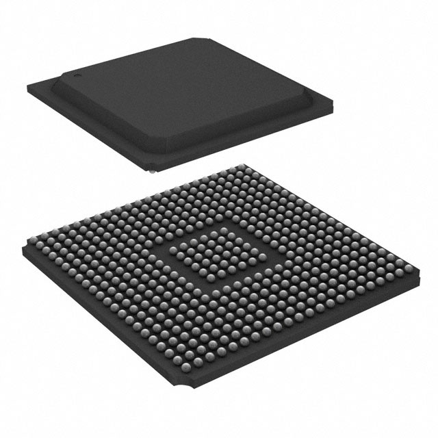
Virtex®-E Field Programmable Gate Array (FPGA) IC 260 114688 5292 352-LBGA Exposed Pad, Metal |
|---|---|
| Quantity | 319 Available (as of October 8, 2026) |

| Product Category | Field Programmable Gate Array (FPGA) |
|---|---|
| Manufacturer | AMD |
| Manufacturing Status | Obsolete |
| Manufacturer Standard Lead Time | Contact Us |
| Datasheet |
Specifications & Environmental
| Device Package | 352-MBGA (35x35) | Grade | Commercial | Operating Temperature | 0°C – 85°C | ||
|---|---|---|---|---|---|---|---|
| Package / Case | 352-LBGA Exposed Pad, Metal | Number of I/O | 260 | Voltage | 1.71 V - 1.89 V | ||
| Mounting Method | Surface Mount | RoHS Compliance | RoHS non-compliant | REACH Compliance | REACH Unaffected | ||
| Moisture Sensitivity Level | 3 (168 Hours) | Number of LABs/CLBs | 1176 | Number of Logic Elements/Cells | 5292 | ||
| Number of Gates | 306393 | ECCN | 3A991D | HTS Code | 8542.39.0001 | ||
| Qualification | N/A | Total RAM Bits | 114688 |
Overview of XCV200E-6BG352C – Virtex®-E FPGA, 352-LBGA
The XCV200E-6BG352C is a Virtex®-E field programmable gate array (FPGA) from AMD supplied in a 352-LBGA exposed pad metal package. It combines on-chip logic, embedded memory, and a high I/O count in a surface-mount package aimed at commercial applications requiring reprogrammable logic and flexible I/O interfacing.
This device is based on the Virtex-E family architecture and is specified for a 1.71–1.89 V core supply with an operating range of 0 °C to 85 °C, making it suitable for a broad set of commercial embedded designs.
Key Features
- Logic Capacity – Approximately 5,292 logic elements and about 306,393 gates for implementing custom logic, glue, and accelerator functions.
- Embedded Memory – Approximately 0.115 Mbits (114,688 bits) of on-chip RAM to support buffering, FIFOs, and small data stores.
- I/O Density – 260 available I/O pins to support multiple parallel interfaces and high pin-count designs.
- Power and Supply – Core voltage supply specified at 1.71 V to 1.89 V for the internal FPGA logic.
- Package and Mounting – 352-LBGA exposed pad, metal package (supplier device package: 352-MBGA, 35×35) designed for surface-mount assembly.
- Temperature and Grade – Commercial-grade device with an operating temperature range of 0 °C to 85 °C.
- RoHS Compliance – Device is RoHS compliant.
- Virtex‑E Family Features (series-level) – Family-level capabilities include 1.8 V FPGA architecture, SelectI/O+ interface flexibility, differential signalling support (e.g., LVDS, BLVDS, LVPECL), SelectRAM+ memory hierarchy, multiple DLLs for clock management, SRAM-based in-system configuration, and advanced packaging options as documented for the Virtex‑E series.
Typical Applications
- Communications and Networking – Use the device’s high I/O count and Virtex‑E family differential signalling support to implement protocol bridging, packet processing, and custom interface logic.
- High‑Speed Interfaces – Implement memory controllers, interface adaptors, and source-synchronous links taking advantage of on-chip memory and clock-management features described for Virtex‑E devices.
- Custom Logic and Glue – Replace ASIC or discrete logic with reprogrammable FPGA logic for application-specific control, glue logic, and pre-production prototypes.
- Embedded Processing and DSP – Deploy as a platform for embedded accelerators, parallel datapaths, and signal-processing blocks using available logic and embedded RAM.
Unique Advantages
- Balanced Logic and Memory – A combination of ~5,292 logic elements and ~114,688 bits of on-chip RAM supports mid-density designs that require both logic and local storage.
- High Pin Count – 260 I/Os enable broad connectivity to peripherals, memory devices, and high-speed interfaces without external multiplexing.
- Commercial Temperature Range – Rated 0 °C to 85 °C to meet typical commercial embedded system requirements.
- Surface-Mount 352-LBGA Package – A compact, metal-exposed pad BGA package suitable for modern PCB assembly and thermal dissipation strategies.
- RoHS Compliant – Registered for RoHS compliance to support environmental and regulatory requirements.
- Family-Level Clock and I/O Capabilities – Leveraging Virtex‑E family features (multiple DLLs, flexible SelectI/O+ standards, differential signalling) simplifies system-level timing and interface design.
Why Choose XCV200E-6BG352C?
The XCV200E-6BG352C offers a mid-density Virtex‑E FPGA option that brings together reprogrammable logic, embedded RAM, and substantial I/O resources in a 352-LBGA surface-mount package. Its 1.71–1.89 V core supply, commercial temperature rating, and RoHS compliance make it appropriate for a wide range of commercial embedded designs where flexibility and reconfigurability are required.
This device is well suited to engineering teams designing communication interfaces, custom accelerators, or integration platforms that benefit from in-system reprogramming and the Virtex‑E family’s documented clock and memory management features. It provides a practical balance of integration and performance for scalable, maintainable designs backed by the Virtex‑E documentation set.
Request a quote or submit an inquiry to get pricing and availability details for XCV200E-6BG352C. Our team can provide lead-time information and support for your procurement and design planning needs.























Date Founded: 1969
Headquarters: Santa Clara, California, USA
Employees: 25,000+
Revenue: $22.68 Billion
Certifications and Memberships: ISO9001:2015, RoHS, REACH











