
XCV2000E-8FG680C
| Part Description |
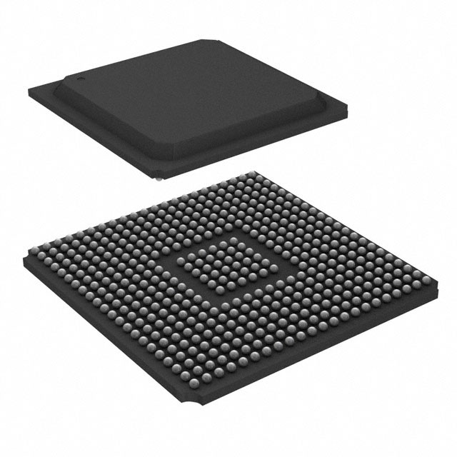
Virtex®-E Field Programmable Gate Array (FPGA) IC 512 655360 43200 680-LBGA Exposed Pad |
|---|---|
| Quantity | 912 Available (as of October 7, 2026) |

| Product Category | Field Programmable Gate Array (FPGA) |
|---|---|
| Manufacturer | AMD |
| Manufacturing Status | Obsolete |
| Manufacturer Standard Lead Time | Contact Us |
| Datasheet |
Specifications & Environmental
| Device Package | 680-FTEBGA (40x40) | Grade | Commercial | Operating Temperature | 0°C – 85°C | ||
|---|---|---|---|---|---|---|---|
| Package / Case | 680-LBGA Exposed Pad | Number of I/O | 512 | Voltage | 1.71 V - 1.89 V | ||
| Mounting Method | Surface Mount | RoHS Compliance | RoHS non-compliant | REACH Compliance | REACH Unaffected | ||
| Moisture Sensitivity Level | 3 (168 Hours) | Number of LABs/CLBs | 9600 | Number of Logic Elements/Cells | 43200 | ||
| Number of Gates | 2541952 | ECCN | 3A001A7A | HTS Code | 8542.39.0001 | ||
| Qualification | N/A | Total RAM Bits | 655360 |
Overview of XCV2000E-8FG680C – Virtex®-E FPGA, 512 I/Os, approximately 0.66 Mbits embedded RAM
The XCV2000E-8FG680C is a Virtex®-E field programmable gate array (FPGA) in a 680-LBGA exposed pad package targeted at commercial-temperature designs. It combines a high logic element count with substantial on-chip memory and a broad, flexible I/O set, enabling complex digital system integration for high-performance interface, processing and memory-bridging applications.
Key Features
- Core logic Up to 43,200 logic elements (logic cells) and approximately 2,541,952 system gates provide the combinational and sequential resources for complex logic designs.
- Configurable memory Approximately 0.66 Mbits of total on-chip RAM and support for block and distributed RAM structures for data buffering and on-chip storage.
- I/O density and flexibility 512 user I/Os with SelectI/O+™ technology supporting a wide range of interface standards and differential signalling options including LVDS, BLVDS and LVPECL.
- High-speed interfacing Family-level support for PCI-compliant 3.3 V 32/64-bit operation at 33/66 MHz and double-data-rate link options for high-bandwidth system links.
- Clock management Multiple digital DLLs and clock management features enable frequency multiplication, divide and duty-cycle synthesis suitable for synchronous, high-speed designs.
- Performance and process Designed on a 0.18 µm, 6-layer metal process with internal performance targets noted at family-level (e.g., 130 MHz internal performance for four LUT levels).
- Power and supply Internal supply (VCCINT) specified at 1.71 V to 1.89 V for the device core; I/O supplies are designed to support multiple I/O standards.
- Package and mounting 680-ball FTE BGA (40 × 40 mm) with exposed pad, surface-mount package for board-level thermal performance and dense integration.
- Operating grade and compliance Commercial temperature range of 0 °C to 85 °C and RoHS-compliant construction.
Typical Applications
- High-speed interface bridging Implement PCI and other parallel/serial protocol bridges leveraging the device’s PCI compliance and flexible I/O standards support.
- Memory controller and buffering Use the on-chip block and distributed RAM resources to implement controllers and buffering for external memory interfaces.
- High-performance digital signal processing Deploy the abundant logic elements and dedicated arithmetic/carry resources for DSP pipelines and complex bit-manipulation tasks.
- Multi-standard I/O conversion Integrate LVDS, BLVDS and LVPECL signaling for systems requiring mixed signaling and high aggregate bandwidth.
Unique Advantages
- High logic capacity: 43,200 logic elements enable large-scale designs and substantial functional integration on a single device.
- Significant embedded memory: Approximately 0.66 Mbits of on-chip RAM reduces dependence on external memory for many buffering and scratchpad needs.
- Flexible, high-density I/O: 512 I/Os with SelectI/O+ support a wide set of signaling standards to simplify interfacing with legacy and high-speed peripherals.
- Comprehensive clocking: Multiple digital DLLs and clock synthesis features enable robust timing architectures for high-speed systems.
- Compact, manufacturable package: 680‑LBGA exposed pad surface-mount package supports dense PCB routing and thermal contact for power-dissipation needs.
- Regulatory and process consistency: 0.18 µm process design and RoHS compliance support continuity across production and environmental requirements.
Why Choose XCV2000E-8FG680C?
The XCV2000E-8FG680C positions itself as a high-capacity Virtex®-E FPGA option for designers who need a blend of large logic resources, on-chip memory, and flexible high-speed I/O in a commercially graded device. Its combination of approximately 43,200 logic elements, substantial embedded RAM, and broad I/O capability makes it suitable for advanced interface bridging, processing acceleration and memory-intensive functions.
For engineering teams seeking a field-programmable solution with proven family-level features—such as SelectI/O+ signaling, multiple clock DLLs, and PCI interoperability—this device offers a strong foundation for building scalable, reprogrammable systems while maintaining standard commercial temperature and power requirements.
Request a quote or submit a parts inquiry to receive pricing, availability and lead-time information for XCV2000E-8FG680C.






















Date Founded: 1969
Headquarters: Santa Clara, California, USA
Employees: 25,000+
Revenue: $22.68 Billion
Certifications and Memberships: ISO9001:2015, RoHS, REACH











