
XCV200E-6FG456I
| Part Description |
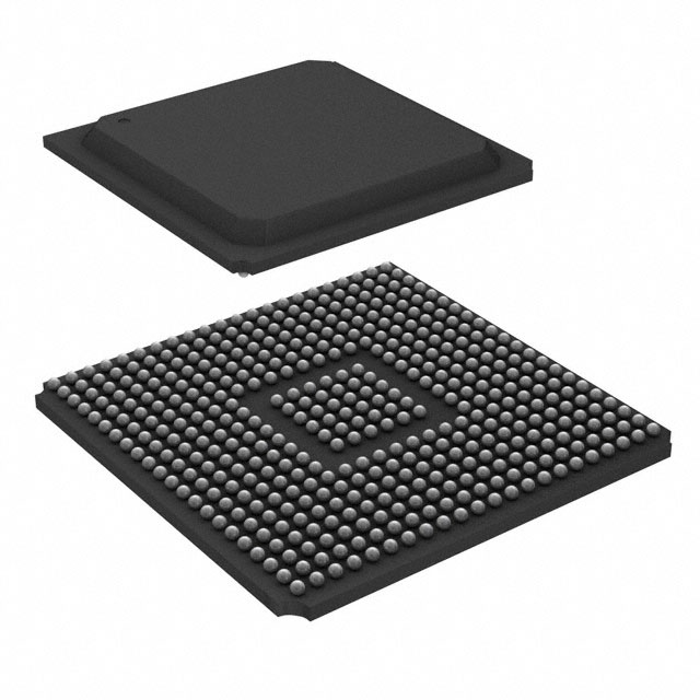
Virtex®-E Field Programmable Gate Array (FPGA) IC 284 114688 5292 456-BBGA |
|---|---|
| Quantity | 1,805 Available (as of June 17, 2026) |

| Product Category | Field Programmable Gate Array (FPGA) |
|---|---|
| Manufacturer | AMD |
| Manufacturing Status | Obsolete |
| Manufacturer Standard Lead Time | Contact Us |
| Datasheet |
Specifications & Environmental
| Device Package | 456-FBGA (23x23) | Grade | Industrial | Operating Temperature | -40°C – 100°C | ||
|---|---|---|---|---|---|---|---|
| Package / Case | 456-BBGA | Number of I/O | 284 | Voltage | 1.71 V - 1.89 V | ||
| Mounting Method | Surface Mount | RoHS Compliance | RoHS non-compliant | REACH Compliance | REACH Unaffected | ||
| Moisture Sensitivity Level | 3 (168 Hours) | Number of LABs/CLBs | 1176 | Number of Logic Elements/Cells | 5292 | ||
| Number of Gates | 306393 | ECCN | 3A991D | HTS Code | 8542.39.0001 | ||
| Qualification | N/A | Total RAM Bits | 114688 |
Overview of XCV200E-6FG456I – Virtex®-E Field Programmable Gate Array (FPGA)
The XCV200E-6FG456I is a Virtex®-E series Field Programmable Gate Array designed for industrial applications that require reprogrammable digital logic, high I/O density, and on-chip memory. This device combines a low-voltage 1.8 V core architecture with abundant I/O and embedded RAM for prototyping, interface bridging, and system integration tasks.
With 5,292 logic elements, 114,688 bits of on-chip RAM, and 284 general-purpose I/Os in a 456-BBGA package, the part delivers a balance of integration and flexibility for medium-density FPGA designs operating across an industrial temperature range.
Key Features
- Core Logic — 5,292 logic elements provide the programmable fabric for custom logic, state machines, and control functions; device contains approximately 306,393 gates.
- Configurable Memory — 114,688 total RAM bits of embedded memory (≈0.11 Mbit) for buffering, FIFOs, and local data storage.
- I/O Density & Flexibility — 284 user I/Os to support extensive external connectivity and high pin-count peripheral interfaces.
- Package & Mounting — 456-ball BGA (supplier package: 456-FBGA, 23×23) in a surface-mount form factor for compact board-level integration.
- Voltage & Power — Core supply range specified at 1.71 V to 1.89 V (1.8 V class device).
- Industrial Temperature Range — Rated for operation from −40 °C to 100 °C to meet demanding environmental conditions.
- SRAM-Based In-System Configuration — Reprogrammable configuration memory enables design iteration and in-field updates.
- Standards & Interfaces (family-level) — Virtex‑E family features noted in the datasheet include high-performance SelectI/O technology, differential signaling support (LVDS, BLVDS, LVPECL), and PCI-compliant operation for relevant devices in the family.
- Compliance — RoHS-compliant manufacturing.
Typical Applications
- High-Speed Interface Bridge — Use the device’s large I/O count and differential signaling support to implement protocol translation and interface bridging between high-speed peripherals and system logic.
- Memory Interface and Controllers — On-chip RAM and the Virtex‑E family’s memory hierarchy support designs requiring local buffering and external memory interfacing.
- Industrial Control and Automation — Industrial-grade temperature rating and surface-mount BGA packaging make the FPGA suitable for control logic, motor control interfaces, and factory automation systems.
- Prototyping and System Integration — Reprogrammable SRAM configuration enables iterative development, algorithm validation, and system-level integration before production.
Unique Advantages
- Balanced Integration: 5,292 logic elements with on-chip RAM reduce the need for external glue logic and memory in mid-density designs.
- High I/O Count: 284 I/Os provide the pin budget necessary for complex peripheral and sensor interfacing without adding external multiplexing logic.
- Industrial Readiness: Qualified to operate from −40 °C to 100 °C, supporting reliable operation in harsh environments.
- Flexible Packaging: 456-ball BGA (23×23) enables dense board layouts while maintaining a compact footprint for space-constrained systems.
- Reconfigurability: SRAM-based, in-system reprogrammability enables design updates and field upgrades to extend product lifecycles.
- Standards-Compatible (family-level): Family features include support for PCI and multiple differential I/O standards, facilitating integration with a range of external devices and buses.
Why Choose XCV200E-6FG456I?
The XCV200E-6FG456I offers a practical combination of logic capacity, embedded RAM, and high I/O count in an industrial-temperature FPGA package. It suits engineering teams that need a reprogrammable, medium-density FPGA to implement interface logic, memory buffering, and system control functions while keeping board BOM and complexity under control.
Backed by the Virtex‑E family’s design ecosystem and SRAM-based in-system configuration, this device supports iterative development and long-term design flexibility for applications where reliability, integration, and reprogrammability are priorities.
Request a quote or submit a pricing and availability inquiry to proceed with procurement or to get more technical details for your design planning.


Date Founded: 1969
Headquarters: Santa Clara, California, USA
Employees: 25,000+
Revenue: $22.68 Billion
Certifications and Memberships: ISO9001:2015, RoHS, REACH


