
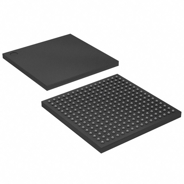
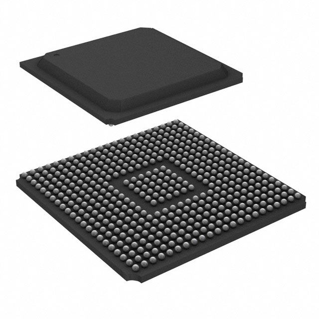
XCV300E-7PQ240C
| Part Description |
Virtex®-E Field Programmable Gate Array (FPGA) IC 158 131072 6912 240-BFQFP |
|---|---|
| Quantity | 1,019 Available (as of June 15, 2026) |

| Product Category | Field Programmable Gate Array (FPGA) |
|---|---|
| Manufacturer | AMD |
| Manufacturing Status | Obsolete |
| Manufacturer Standard Lead Time | Contact Us |
| Datasheet |
Specifications & Environmental
| Device Package | 240-PQFP (32x32) | Grade | Commercial | Operating Temperature | 0°C – 85°C | ||
|---|---|---|---|---|---|---|---|
| Package / Case | 240-BFQFP | Number of I/O | 158 | Voltage | 1.71 V - 1.89 V | ||
| Mounting Method | Surface Mount | RoHS Compliance | RoHS non-compliant | REACH Compliance | REACH Unaffected | ||
| Moisture Sensitivity Level | 3 (168 Hours) | Number of LABs/CLBs | 1536 | Number of Logic Elements/Cells | 6912 | ||
| Number of Gates | 411955 | ECCN | 3A001A7B | HTS Code | 8542.39.0001 | ||
| Qualification | N/A | Total RAM Bits | 131072 |
Overview of XCV300E-7PQ240C – Virtex®-E FPGA, 240-BFQFP, 158 I/O
The XCV300E-7PQ240C is an AMD Virtex®-E family field programmable gate array provided in a 240-BFQFP (240-PQFP, 32×32) surface-mount package. It delivers a mid-density SRAM-based FPGA architecture with 6,912 logic elements, 158 user I/Os and on-chip memory resources suited for designs requiring flexible high-speed I/O and embedded memory.
Built on the Virtex‑E family architecture, the device targets applications that benefit from high-performance interfaces, configurable on-chip RAM and integrated clock management while operating from a 1.71 V to 1.89 V core supply and within a commercial temperature range of 0 °C to 85 °C.
Key Features
- Logic Capacity — 6,912 logic elements supporting complex combinational and sequential logic implementation.
- Embedded Memory — 131,072 bits of total on-chip RAM (approximately 0.13 Mbits) for distributed and block RAM usage.
- I/O — 158 user I/Os provided in the 240‑BFQFP package for broad interface connectivity.
- Gate Equivalent — Device density reported at 411,955 gates for system-level resource planning.
- Power and Supply — Core voltage supply range of 1.71 V to 1.89 V for the internal logic and memory.
- Package & Mounting — Supplied in a 240‑BFQFP (240‑PQFP, 32×32) surface-mount package; supplier device package listed as 240‑PQFP (32×32).
- Commercial Grade — Operating temperature range 0 °C to 85 °C; RoHS compliant.
- Virtex‑E Family Capabilities (series-level) — Family features include 1.8 V operation, SelectI/O+ interface flexibility, differential signalling support (LVDS, BLVDS, LVPECL), an advanced SelectRAM+ memory hierarchy, built-in digital clock management with multiple DLLs, and SRAM-based in-system configuration.
Typical Applications
- High-Speed Interface Design — Implements source-synchronous and differential interfaces using the Virtex‑E series’ SelectI/O+ and differential signalling support for demanding link requirements.
- Memory Interface Controllers — Suited for designs requiring tight integration with external memories, benefiting from the family’s SelectRAM+ memory hierarchy and on-chip RAM resources.
- FPGA-Based System Prototyping — Provides re-programmability and a substantial logic/memory mix for iterative development and in-system configuration workflows.
- Clock-Intensive Designs — Integrates multiple digital DLLs for clock multiplication, division and duty-cycle control in timing-sensitive applications.
Unique Advantages
- Balanced Logic and Memory: 6,912 logic elements combined with approximately 0.13 Mbits of on-chip RAM allow compact implementations of control, datapath and buffering functions without excessive external memory.
- Flexible I/O Options: 158 user I/Os in the 240‑BFQFP package support a wide range of interface needs, including differential signaling standards at the family level.
- Integrated Clock Management: Family-level digital DLLs enable precise clocking and DDR-friendly duty-cycle control, simplifying high-speed timing design.
- SRAM-Based Re-programmability: In-system configurability enables design updates and iterative development without hardware replacement.
- Compact, Surface-Mount Package: The 240‑BFQFP (240‑PQFP, 32×32) surface-mount form factor supports board-level density and manufacturability.
- Regulatory & Manufacturing Readiness: Commercial-grade temperature rating and RoHS compliance support mainstream production and procurement.
Why Choose XCV300E-7PQ240C?
The XCV300E-7PQ240C positions itself as a versatile mid-density Virtex‑E FPGA option where a combination of logic capacity, embedded RAM and flexible high-speed I/O is required. Its family-level capabilities—SelectI/O+, SelectRAM+ memory architecture and integrated clock management—align with designs that need reliable in-system configurability and robust timing control.
This device is well suited to engineering teams building communications, memory-interface, or prototype FPGA designs that require a commercial-grade, RoHS-compliant solution in a compact 240‑BFQFP package. The combination of on-chip memory, substantial logic elements and programmable I/O simplifies system integration and supports iterative development cycles.
Request a quote or submit a pricing and availability inquiry for XCV300E-7PQ240C to receive current lead-time and ordering information.


Date Founded: 1969
Headquarters: Santa Clara, California, USA
Employees: 25,000+
Revenue: $22.68 Billion
Certifications and Memberships: ISO9001:2015, RoHS, REACH


