
XCV300E-8BG432C
| Part Description |
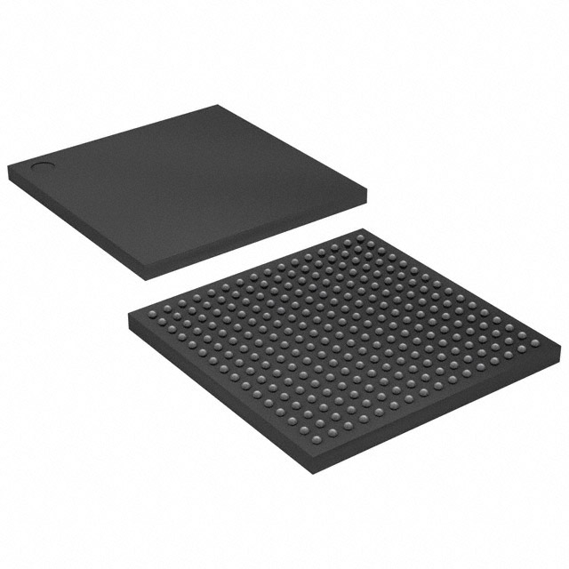
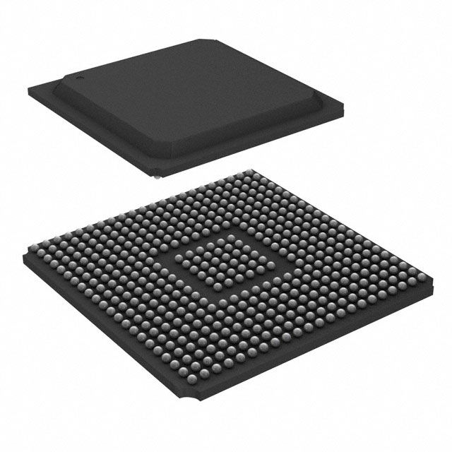
Virtex®-E Field Programmable Gate Array (FPGA) IC 316 131072 6912 432-LBGA Exposed Pad, Metal |
|---|---|
| Quantity | 396 Available (as of June 15, 2026) |

| Product Category | Field Programmable Gate Array (FPGA) |
|---|---|
| Manufacturer | AMD |
| Manufacturing Status | Obsolete |
| Manufacturer Standard Lead Time | Contact Us |
| Datasheet |
Specifications & Environmental
| Device Package | 432-MBGA (40x40) | Grade | Commercial | Operating Temperature | 0°C – 85°C | ||
|---|---|---|---|---|---|---|---|
| Package / Case | 432-LBGA Exposed Pad, Metal | Number of I/O | 316 | Voltage | 1.71 V - 1.89 V | ||
| Mounting Method | Surface Mount | RoHS Compliance | RoHS non-compliant | REACH Compliance | REACH Unaffected | ||
| Moisture Sensitivity Level | 3 (168 Hours) | Number of LABs/CLBs | 1536 | Number of Logic Elements/Cells | 6912 | ||
| Number of Gates | 411955 | ECCN | 3A991D | HTS Code | 8542.39.0001 | ||
| Qualification | N/A | Total RAM Bits | 131072 |
Overview of XCV300E-8BG432C – Virtex®-E Field Programmable Gate Array (FPGA) IC, 432-LBGA
The XCV300E-8BG432C is a Virtex®-E family FPGA providing high-density, reprogrammable logic in a 432-LBGA exposed-pad package. This commercial-grade, surface-mount device delivers programmable logic, on-chip memory, and extensive I/O suitable for system-level designs requiring flexible interface support and programmable functionality.
Its architecture targets applications that need substantial logic resources, abundant I/O, and integrated memory while operating from a 1.71 V to 1.89 V core supply and a commercial temperature range of 0 °C to 85 °C.
Key Features
- Logic Resources — 6,912 logic elements (reported equivalent to 411,955 gates), providing the programmable fabric needed for complex digital functions.
- Configurable Logic Blocks — Architecture includes 1,536 logic blocks (CLBs) to implement combinational and sequential logic structures.
- Embedded Memory — Approximately 0.125 Mbits of on-chip RAM (131,072 total RAM bits) for buffering, state storage, and small on-chip data structures.
- I/O Capacity — Up to 316 I/O pins to support wide parallel interfaces and multiple external devices.
- Power and Supply — Core voltage specified at 1.71 V to 1.89 V to match the Virtex-E 1.8 V class device requirements.
- Package and Mounting — 432-LBGA exposed pad, metal package (supplier package: 432-MBGA, 40×40) for surface-mount assembly.
- Operating Range — Commercial grade device rated for 0 °C to 85 °C operation.
- Standards and Family Features — As a Virtex-E family device, benefits include high-speed I/O standards, differential signalling support, multiple DLLs for clock management, and in-system reprogrammability (as described in the Virtex-E family documentation).
- Compliance — RoHS compliant.
Typical Applications
- System Prototyping and Development — Use the programmable fabric and on-chip memory to prototype complex digital subsystems and iterate hardware designs quickly.
- High-Speed I/O Interfaces — Leverage the large I/O count and Virtex-E family I/O capabilities to implement parallel interfaces, memory controllers, and protocol bridging.
- Communication and Networking — Implement packet processing, protocol adaptation, and custom data-path logic using the device’s logic resources and I/O capacity.
- Embedded Control and Signal Processing — Deploy custom control logic, finite-state machines, and modest signal-processing pipelines using embedded RAM and abundant logic elements.
Unique Advantages
- Substantial Logic Density: 6,912 logic elements provide the capacity to implement complex FPGA designs without external ASICs for many functions.
- Generous I/O Count: 316 I/Os enable broad connectivity to peripherals, memories, and interfaces, reducing the need for external multiplexers or expanders.
- On-Chip Memory: Approximately 0.125 Mbits of embedded RAM supports buffering, lookup tables, and state retention directly on the device.
- Package Flexibility: 432-LBGA exposed-pad, metal construction supports reliable surface-mount assembly and thermal conduction for system integration.
- Commercial Operating Range: Rated for 0 °C to 85 °C to match many standard product and development environments.
- RoHS Compliance: Environmentally compliant status simplifies regulatory and procurement considerations.
Why Choose XCV300E-8BG432C?
The XCV300E-8BG432C positions itself as a capable Virtex-E class FPGA option when designers need a balance of logic capacity, on-chip memory, and extensive I/O in a compact LBGA package. Its specified core voltage range and commercial operating temperature make it suitable for mainstream embedded systems, communication interfaces, and prototype platforms that rely on reprogrammable logic.
For teams building systems that require in-field programmability, broad I/O support, and a proven family architecture, this device offers a concise set of programmable resources and package choices that simplify board-level integration and accelerate development timelines.
Request a quote or submit a product inquiry to evaluate the XCV300E-8BG432C for your next design.


Date Founded: 1969
Headquarters: Santa Clara, California, USA
Employees: 25,000+
Revenue: $22.68 Billion
Certifications and Memberships: ISO9001:2015, RoHS, REACH


