
XCV300E-7FG456I
| Part Description |
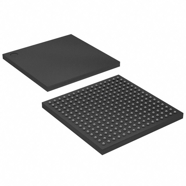
Virtex®-E Field Programmable Gate Array (FPGA) IC 312 131072 6912 456-BBGA |
|---|---|
| Quantity | 871 Available (as of October 8, 2026) |

| Product Category | Field Programmable Gate Array (FPGA) |
|---|---|
| Manufacturer | AMD |
| Manufacturing Status | Obsolete |
| Manufacturer Standard Lead Time | Contact Us |
| Datasheet |
Specifications & Environmental
| Device Package | 456-FBGA (23x23) | Grade | Industrial | Operating Temperature | -40°C – 100°C | ||
|---|---|---|---|---|---|---|---|
| Package / Case | 456-BBGA | Number of I/O | 312 | Voltage | 1.71 V - 1.89 V | ||
| Mounting Method | Surface Mount | RoHS Compliance | RoHS non-compliant | REACH Compliance | REACH Unaffected | ||
| Moisture Sensitivity Level | 3 (168 Hours) | Number of LABs/CLBs | 1536 | Number of Logic Elements/Cells | 6912 | ||
| Number of Gates | 411955 | ECCN | 3A991D | HTS Code | 8542.39.0001 | ||
| Qualification | N/A | Total RAM Bits | 131072 |
Overview of XCV300E-7FG456I – Virtex®-E Field Programmable Gate Array (FPGA) IC 312 131072 6912 456-BBGA
The XCV300E-7FG456I is a Virtex‑E series 1.8 V SRAM-based FPGA provided in a 456-pin BGA package. It delivers medium-density programmable logic with 6,912 logic elements, approximately 131,072 bits of embedded RAM, and 312 user I/O pins—targeted for industrial-temperature applications.
Designed for reconfigurable system designs, the device combines on-chip memory, a high I/O count and family-level features such as support for high-performance differential signaling and integrated clock management to address a range of embedded, communications and interface tasks.
Key Features
- Programmable Logic 6,912 logic elements and approximately 411,955 gates of logic capacity for implementing glue logic, protocol engines, and custom datapaths.
- On-Chip Memory Approximately 131,072 bits of embedded RAM for local buffering, FIFOs and small on-chip storage requirements.
- I/O and Interface Capability 312 user I/O pins in a 456-pin BGA footprint; family-level SelectI/O+ technology supports a wide range of single‑ended and differential I/O standards for high-speed interface flexibility.
- Clock Management Family features include multiple digitally implemented DLLs for clock multiply/divide and duty-cycle control to support synchronous designs and DDR-style interfaces.
- Power and Supply Core supply operation specified from 1.71 V to 1.89 V (1.8 V nominal), enabling compatibility with Virtex‑E family power domains.
- Packaging and Mounting Delivered in a 456-ball BGA package (supplier device package 456-FBGA, 23×23) for surface-mount PCB assembly and high-density board layouts.
- Industrial Temperature Grade Qualified for operation from −40 °C to 100 °C for deployment in industrial environments.
- Configuration Model SRAM-based in‑system configuration enables unlimited reprogramming for iterative development and field updates.
- Compliance and Testing RoHS compliant and produced under family test regimes that include 100% factory testing.
Typical Applications
- High‑speed interface bridging Implement protocol conversion, parallel-to-serial bridging and custom interface logic using the device’s high I/O count and family-level differential signaling support.
- Embedded control and glue logic Consolidate discrete logic, timers and control functions into reconfigurable logic blocks to simplify BOM and speed development.
- Industrial data acquisition and preprocessing Use on-chip RAM and programmable logic to buffer, align and preprocess sensor or fieldbus data within an industrial temperature range.
Unique Advantages
- Balanced medium-density resource set 6,912 logic elements and ~131 Kbits of embedded RAM provide a practical mix of logic and memory for mid-range FPGA tasks without overprovisioning.
- High I/O count in a compact BGA 312 I/Os in a 456-pin BGA enable complex I/O routing while maintaining a compact PCB footprint.
- Industrial operating range Rated from −40 °C to 100 °C to meet temperature requirements for industrial deployments.
- Reprogrammable SRAM configuration In-system reprogramming supports iterative development, field upgrades and multi‑function product designs.
- Precise core supply specification Core voltage range of 1.71–1.89 V helps ensure consistent device behavior across boards and power architectures.
- Production-level quality controls RoHS compliance and 100% factory testing provide traceable manufacturing quality for system integration.
Why Choose XCV300E-7FG456I?
The XCV300E-7FG456I positions itself as a practical Virtex‑E option for designers who need a medium-density, industrial-temperature FPGA with a robust set of I/O and on-chip memory. Its combination of 6,912 logic elements, approximately 131 Kbits of embedded RAM and 312 I/Os in a 456-ball BGA makes it suitable for embedded control, interface bridging and industrial data handling.
With SRAM-based in-system configuration, established family-level capabilities for differential signaling and clock management, and defined supply and temperature specifications, this part supports iterative development cycles and deployed systems that require reconfigurability and industrial-grade operation.
Request a quote or submit a purchase inquiry to receive pricing and availability for XCV300E-7FG456I. Include required quantities and any application or packaging notes to accelerate response time.
























Date Founded: 1969
Headquarters: Santa Clara, California, USA
Employees: 25,000+
Revenue: $22.68 Billion
Certifications and Memberships: ISO9001:2015, RoHS, REACH











