
XCVU080-2FFVB2104E
| Part Description |
Virtex® UltraScale™ Field Programmable Gate Array (FPGA) IC 702 51200000 975000 2104-BBGA, FCBGA |
|---|---|
| Quantity | 506 Available (as of June 15, 2026) |

| Product Category | Field Programmable Gate Array (FPGA) |
|---|---|
| Manufacturer | AMD |
| Manufacturing Status | Active |
| Manufacturer Standard Lead Time | 16 Weeks |
| Datasheet |
Specifications & Environmental
| Device Package | 2104-FCBGA (47.5x47.5) | Grade | Extended | Operating Temperature | 0°C – 100°C | ||
|---|---|---|---|---|---|---|---|
| Package / Case | 2104-BBGA, FCBGA | Number of I/O | 702 | Voltage | 922 mV - 979 mV | ||
| Mounting Method | Surface Mount | RoHS Compliance | ROHS3 Compliant | REACH Compliance | REACH Unaffected | ||
| Moisture Sensitivity Level | 4 (72 Hours) | Number of LABs/CLBs | 55714 | Number of Logic Elements/Cells | 975000 | ||
| Number of Gates | N/A | ECCN | 3A001A7B | HTS Code | 8542.39.0001 | ||
| Qualification | N/A | Total RAM Bits | 51200000 |
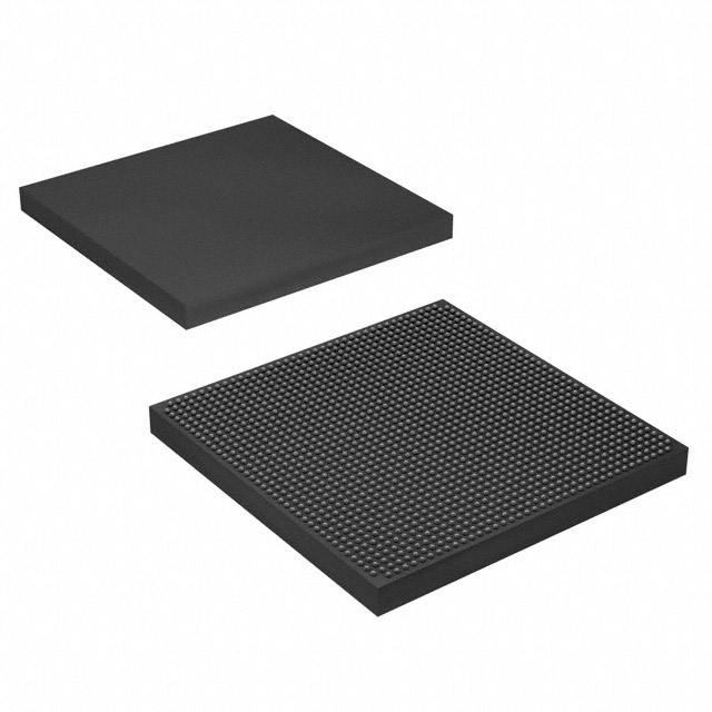
Overview of XCVU080-2FFVB2104E – Virtex® UltraScale™ FPGA, 975,000 logic elements, 2104-FCBGA
The XCVU080-2FFVB2104E is a Virtex® UltraScale™ field programmable gate array (FPGA) IC from AMD. It delivers high logic capacity, substantial embedded memory, and a large I/O complement in a 2104-ball FCBGA package for surface-mount applications.
With 975,000 logic elements, approximately 51.2 Mbits of embedded RAM, and 702 I/O pins, this device is intended for designs that require dense programmable logic, significant on-chip memory, and extensive external connectivity while operating within the specified supply and temperature ranges.
Key Features
- Logic Capacity Contains 975,000 logic elements to support complex, high-density logic implementations.
- Configurable Logic Blocks Built with 55,714 CLBs to organize and structure programmable logic resources across designs.
- Embedded Memory Approximately 51.2 Mbits of on-chip RAM for buffering, FIFOs, and local storage of intermediate data.
- I/O Density 702 I/O pins provide broad external connectivity for multi-channel interfaces and large system integrations.
- Package 2104-BBGA / 2104-FCBGA package (2104-FCBGA (47.5x47.5)) optimized for high-pin-count surface-mount mounting.
- Power Specified operating core voltage range from 922 mV to 979 mV to match system power-rail requirements.
- Operating Range Grade: Extended. Rated for operation from 0 °C to 100 °C for a range of commercial and extended-temperature applications.
- Mounting and Compliance Surface-mount device with RoHS compliance for lead-free assembly processes.
Typical Applications
- High-density digital signal processing Leverage the large logic element count and embedded RAM for compute-heavy signal processing pipelines and stream processing tasks.
- Multi-channel interface aggregation Use the 702 I/O pins to aggregate and manage numerous high-pin-count interfaces in communication and networking equipment.
- Complex control and instrumentation Implement sophisticated control logic and local data buffering where significant on-chip memory and logic resources reduce external component count.
Unique Advantages
- High logic density: 975,000 logic elements enable implementation of large-scale, integrated FPGA designs without partitioning across multiple devices.
- Substantial embedded memory: Approximately 51.2 Mbits of RAM supports deep buffering and on-chip data handling to minimize external memory dependency.
- Extensive I/O availability: 702 I/O pins allow flexible connectivity for multi-channel systems, reducing the need for external I/O expanders.
- Compact high-pin-count package: The 2104-FCBGA form factor consolidates many signals in a single surface-mount package for dense board layouts.
- Controlled power window: Operation across a defined 922 mV–979 mV supply range aids predictable power design and regulation planning.
- RoHS-compliant and extended grade: Ready for lead-free assembly and rated for extended operating temperatures to fit a variety of system environments.
Why Choose XCVU080-2FFVB2104E?
The XCVU080-2FFVB2104E positions itself as a high-capacity FPGA solution that balances large programmable logic resources, significant on-chip RAM, and a broad I/O complement in a single 2104-ball FCBGA surface-mount package. Its specified voltage and temperature ranges, combined with RoHS compliance and extended-grade rating, make it suitable for engineers targeting dense, I/O-rich FPGA implementations.
This device is well suited to teams developing complex digital systems that require on-chip memory, high logic density, and many external interfaces, offering a scalable platform for consolidating system functions and reducing external component count.
Request a quote or submit an inquiry for pricing and availability of the XCVU080-2FFVB2104E to evaluate its fit for your next high-density FPGA design.


Date Founded: 1969
Headquarters: Santa Clara, California, USA
Employees: 25,000+
Revenue: $22.68 Billion
Certifications and Memberships: ISO9001:2015, RoHS, REACH


