
XCVU095-2FFVC2104E
| Part Description |
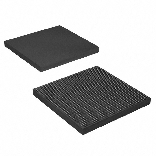
Virtex® UltraScale™ Field Programmable Gate Array (FPGA) IC 416 62259200 1176000 2104-BBGA, FCBGA |
|---|---|
| Quantity | 761 Available (as of June 15, 2026) |

| Product Category | Field Programmable Gate Array (FPGA) |
|---|---|
| Manufacturer | AMD |
| Manufacturing Status | Active |
| Manufacturer Standard Lead Time | 16 Weeks |
| Datasheet |
Specifications & Environmental
| Device Package | 2104-FCBGA (47.5x47.5) | Grade | Extended | Operating Temperature | 0°C – 100°C | ||
|---|---|---|---|---|---|---|---|
| Package / Case | 2104-BBGA, FCBGA | Number of I/O | 416 | Voltage | 922 mV - 979 mV | ||
| Mounting Method | Surface Mount | RoHS Compliance | ROHS3 Compliant | REACH Compliance | REACH Unaffected | ||
| Moisture Sensitivity Level | 4 (72 Hours) | Number of LABs/CLBs | 67200 | Number of Logic Elements/Cells | 1176000 | ||
| Number of Gates | N/A | ECCN | 3A001A7B | HTS Code | 8542.39.0001 | ||
| Qualification | N/A | Total RAM Bits | 62259200 |
Overview of XCVU095-2FFVC2104E – Virtex® UltraScale™ Field Programmable Gate Array (FPGA) IC 416 62259200 1176000 2104-BBGA, FCBGA
The XCVU095-2FFVC2104E is a Virtex® UltraScale™ FPGA from AMD provided in a 2104-BBGA FCBGA package. It delivers a high-density programmable logic fabric with substantial on-chip memory and a large complement of I/O for complex digital designs.
Designed for surface-mount applications, this device supports an extended temperature grade and operates from a core supply range of 922 mV to 979 mV, making it suitable for demanding board-level implementations that require a compact, high-capacity programmable device.
Key Features
- Programmable Logic Capacity — 1,176,000 logic elements provide significant capacity for large-scale logic integration and parallel processing architectures.
- Embedded Memory — Approximately 62.26 Mbits of on-chip RAM enable extensive buffering, lookup tables, and data storage directly within the FPGA fabric.
- I/O Resources — 416 I/O pins support broad connectivity options for high-pin-count system designs and multiple peripheral interfaces.
- Power and Supply — Operates with a core supply range of 922 mV to 979 mV, allowing designers to plan power delivery and sequencing around a defined voltage window.
- Package and Mounting — Supplied in a 2104-FCBGA package (47.5 × 47.5 mm) for surface-mount assembly, enabling dense board-level integration.
- Operating Range and Grade — Extended grade device specified for an ambient operating range of 0 °C to 100 °C.
- Environmental Compliance — RoHS compliant.
Typical Applications
- Telecommunications — High logic density and large embedded memory support data-path implementations and protocol handling where on-chip resources reduce external component needs.
- Data Center and Acceleration — Dense logic and abundant I/O make the device suitable for hardware acceleration, algorithm implementation, and platform-level integration.
- High-Performance Computing — Large on-chip RAM and significant logic capacity enable complex compute kernels and custom processing pipelines within a single FPGA package.
Unique Advantages
- High Logic Density: 1,176,000 logic elements allow consolidation of large designs into one device, simplifying board layout and interconnect complexity.
- Substantial Embedded Memory: Approximately 62.26 Mbits of on-chip RAM reduce dependence on external memory for buffering and table storage.
- Ample I/O Count: 416 I/Os provide flexibility for connecting multiple interfaces, sensors, and high-pin-count subsystems directly to the FPGA.
- Compact FCBGA Packaging: The 2104-FCBGA (47.5 × 47.5 mm) package supports high-density PCB integration while maintaining a large resource set.
- Defined Supply Window: Core operation within 922 mV to 979 mV allows predictable power design and voltage planning.
- Extended Temperature Grade: Rated for 0 °C to 100 °C operation to meet a range of board- and system-level thermal environments.
Why Choose XCVU095-2FFVC2104E?
The XCVU095-2FFVC2104E positions itself as a high-capacity Virtex® UltraScale™ FPGA option combining over a million logic elements, tens of megabits of embedded RAM, and hundreds of I/Os in a single 2104-FCBGA package. Its specified supply range and extended operating temperature make it appropriate for complex, high-density designs that require substantial on-chip resources.
This device is well suited to designers and teams developing large-scale digital systems that demand integrated memory and extensive I/O without partitioning functionality across multiple devices. The combination of programmable logic, memory, and package density supports scalable designs and streamlined board integration.
Request a quote or submit an inquiry to receive pricing and availability information tailored to your project requirements.


Date Founded: 1969
Headquarters: Santa Clara, California, USA
Employees: 25,000+
Revenue: $22.68 Billion
Certifications and Memberships: ISO9001:2015, RoHS, REACH


