
XCVU11P-1FLGA2577E
| Part Description |
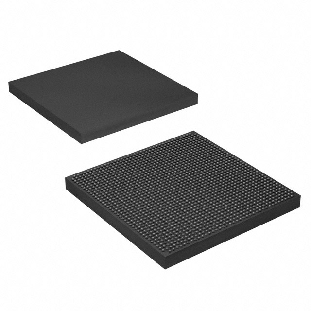
Virtex® UltraScale+™ Field Programmable Gate Array (FPGA) IC 448 396150400 2835000 2577-BBGA, FCBGA |
|---|---|
| Quantity | 1,735 Available (as of June 15, 2026) |

| Product Category | Field Programmable Gate Array (FPGA) |
|---|---|
| Manufacturer | AMD |
| Manufacturing Status | Active |
| Manufacturer Standard Lead Time | 20 Weeks |
| Datasheet |
Specifications & Environmental
| Device Package | 2577-FCBGA (52.5x52.5) | Grade | Extended | Operating Temperature | 0°C – 100°C | ||
|---|---|---|---|---|---|---|---|
| Package / Case | 2577-BBGA, FCBGA | Number of I/O | 448 | Voltage | 825 mV - 876 mV | ||
| Mounting Method | Surface Mount | RoHS Compliance | ROHS3 Compliant | REACH Compliance | REACH Unknown | ||
| Moisture Sensitivity Level | 4 (72 Hours) | Number of LABs/CLBs | 162000 | Number of Logic Elements/Cells | 2835000 | ||
| Number of Gates | N/A | ECCN | 3A001A7B | HTS Code | 8542.39.0001 | ||
| Qualification | N/A | Total RAM Bits | 396150400 |
Overview of XCVU11P-1FLGA2577E – Virtex® UltraScale+™ FPGA, 2577-FCBGA
The XCVU11P-1FLGA2577E is a Virtex® UltraScale+™ field programmable gate array (FPGA) IC from AMD, supplied in a 2577-FCBGA package (52.5 × 52.5 mm). It provides a very large programmable logic capacity and substantial on-chip memory for designs that require significant logic and data storage resources.
With millions of logic elements, hundreds of megabits of embedded RAM and 448 I/O, this device targets applications that need dense integration of programmable logic, high I/O count and broad system interfacing within an extended temperature grade.
Key Features
- Logic Capacity Approximately 2,835,000 logic elements for implementing large-scale digital designs and complex algorithms.
- Embedded Memory Approximately 396 Mbits of on-chip RAM to support buffering, large lookup tables and data-intensive processing.
- I/O Density 448 I/O pins to enable broad peripheral and high-bandwidth system interfacing.
- Supply Voltage Operates from 825 mV to 876 mV, suitable for systems designed around low-voltage core rails.
- Package 2577-BBGA, FCBGA (2577-FCBGA, 52.5 × 52.5 mm) for high-pin-count board designs and thermal/mechanical stability.
- Temperature and Grade Extended grade operation from 0°C to 100°C for deployments requiring a wider commercial temperature range.
- Standards Compliance RoHS compliant, meeting common environmental and material requirements.
Typical Applications
- High-performance compute acceleration Use the large logic and memory resources to implement hardware acceleration for compute-intensive kernels and custom data paths.
- Networking and communications High I/O count and significant on-chip RAM support packet processing, protocol offload and interface bridging.
- Real-time signal and image processing Leverage the device's memory and logic capacity for filtering, encoding/decoding and multi-channel processing pipelines.
- System integration and prototyping Consolidate multiple functions into a single FPGA for board-level integration, rapid prototyping and complex system validation.
Unique Advantages
- Substantial programmable logic: Approximately 2.8 million logic elements reduce the need for multi-chip solutions and simplify system architecture.
- Large on-chip memory: Roughly 396 Mbits of embedded RAM enable local buffering and state storage, improving throughput and latency for data-heavy designs.
- High I/O capability: 448 I/O pins facilitate direct connection to a wide range of peripherals and high-speed interfaces.
- Compact, high-pin-count package: The 2577-FCBGA (52.5 × 52.5 mm) package supports dense routing and thermal management for complex board layouts.
- Extended operating grade: Rated for 0°C to 100°C operation, suitable for applications requiring broader than standard commercial temperature range.
- Regulatory compliance: RoHS compliance supports environmentally-conscious designs and supply chain requirements.
Why Choose XCVU11P-1FLGA2577E?
The XCVU11P-1FLGA2577E combines very large programmable logic capacity, substantial embedded memory and a high I/O count in a single extended-grade FCBGA package. These characteristics make it a strong choice for engineering teams building complex, integrated systems that require on-chip resources for processing, buffering and interfacing.
This device is well suited to designers focused on scalability and consolidation—enabling consolidation of multiple functions into one FPGA and supporting system designs that demand extensive logic, memory and connectivity while operating within a 0°C to 100°C range.
Request a quote or submit an inquiry to receive pricing and availability information for the XCVU11P-1FLGA2577E.


Date Founded: 1969
Headquarters: Santa Clara, California, USA
Employees: 25,000+
Revenue: $22.68 Billion
Certifications and Memberships: ISO9001:2015, RoHS, REACH


