
XCVU11P-1FLGC2104E
| Part Description |
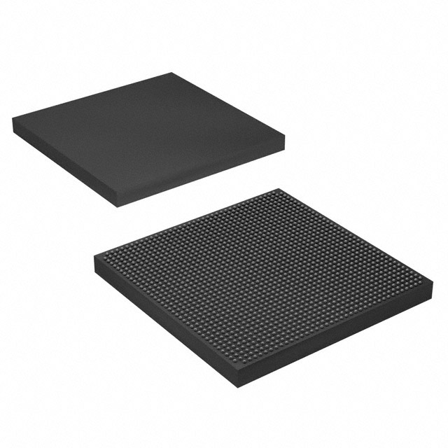
Virtex® UltraScale+™ Field Programmable Gate Array (FPGA) IC 416 396150400 2835000 2104-BBGA, FCBGA |
|---|---|
| Quantity | 1,171 Available (as of June 10, 2026) |

| Product Category | Field Programmable Gate Array (FPGA) |
|---|---|
| Manufacturer | AMD |
| Manufacturing Status | Active |
| Manufacturer Standard Lead Time | 20 Weeks |
| Datasheet |
Specifications & Environmental
| Device Package | 2104-FCBGA (47.5x47.5) | Grade | Extended | Operating Temperature | 0°C – 100°C | ||
|---|---|---|---|---|---|---|---|
| Package / Case | 2104-BBGA, FCBGA | Number of I/O | 416 | Voltage | 825 mV - 876 mV | ||
| Mounting Method | Surface Mount | RoHS Compliance | ROHS3 Compliant | REACH Compliance | REACH Unknown | ||
| Moisture Sensitivity Level | 4 (72 Hours) | Number of LABs/CLBs | 162000 | Number of Logic Elements/Cells | 2835000 | ||
| Number of Gates | N/A | ECCN | 3A001A7B | HTS Code | 8542.39.0001 | ||
| Qualification | N/A | Total RAM Bits | 396150400 |
Overview of XCVU11P-1FLGC2104E – Virtex® UltraScale+™ Field Programmable Gate Array (FPGA), 2104-FCBGA
The XCVU11P-1FLGC2104E is a Virtex® UltraScale+™ FPGA designed for high-bandwidth, system-level integration. Based on the UltraScale+ family architecture, it targets data-intensive applications such as data center networking, wired communications, and waveform processing where large logic capacity and high I/O density are required.
This device combines approximately 2,835,000 logic elements with roughly 396 Mbits of embedded memory, 416 I/O pins and a 2104-FCBGA package (47.5 × 47.5 mm), offering a platform for designs that demand high logic density, large on-chip memory and robust I/O connectivity.
Key Features
- Logic Capacity Approximately 2,835,000 logic elements to implement complex, high-density logic and control functions.
- Embedded Memory Approximately 396 Mbits of on-chip RAM for buffering, LUT-based memory and fast local storage.
- I/O Density 416 I/O pins to support wide parallel interfaces and high pin-count connectivity.
- Power Supply Supported core voltage range of 825 mV to 876 mV, enabling targeted power and performance scaling.
- Package & Mounting 2104-FCBGA package (47.5 × 47.5 mm) in a surface-mount FCBGA form factor for high-pin-count system integration.
- Operating Range Extended-grade device specified for 0 °C to 100 °C ambient operating temperature.
- Standards & Compliance RoHS compliant for regulatory and manufacturing compatibility.
- UltraScale+ Family Capabilities Leverages UltraScale+ architecture benefits including industry-leading performance-per-watt, co-optimization with the Vivado Design Suite, and options in the family such as high-bandwidth memory (HBM) and high-speed serial transceivers for multi-terabit systems (family-level features).
Typical Applications
- Data Center Networking Implement packet processing, traffic management and custom switching logic using high logic capacity and dense I/O.
- Wired Communications Support high-throughput line cards and protocol offload with extensive on-chip memory and high I/O counts.
- Waveform Processing Handle real-time signal processing tasks where large logic resources and embedded RAM are needed for buffering and computation.
- High-Performance Computing Accelerators Deploy custom compute kernels and dataflow architectures using substantial logic and memory resources (family-level DSP and memory capabilities described in the UltraScale+ product brief).
Unique Advantages
- Large Logic Resource Pool: Approximately 2.8 million logic elements let you consolidate complex functions on a single device, reducing board-level component count.
- Significant On-Chip Memory: Approximately 396 Mbits of embedded memory enables large buffering and low-latency data paths without immediate reliance on external DRAM.
- High I/O Pin Count: 416 I/O pins provide the interface density required for wide parallel buses and multi-lane external interfaces.
- Extended-Grade Thermal Range: Specified for 0 °C to 100 °C to support a variety of controlled-environment deployments.
- System-Level Architecture: Built on the UltraScale+ architecture and co-optimized with the Vivado Design Suite, enabling streamlined implementation and design portability within the UltraScale+ family.
- RoHS Compliance: RoHS status simplifies compliance for lead-free assembly and environmental requirements.
Why Choose XCVU11P-1FLGC2104E?
The XCVU11P-1FLGC2104E positions itself as a high-density, system-oriented FPGA option within the Virtex UltraScale+ family. Its large logic element count, substantial embedded memory and high I/O complement designs that require extensive on-chip resources and robust connectivity while maintaining compatibility with the UltraScale+ design ecosystem.
This device is suited for engineering teams building high-throughput, data-centric systems—where consolidation, predictable thermal operation (0 °C to 100 °C), and package-level integration (2104-FCBGA) are key considerations. The family-level features described in the UltraScale+ product brief provide a pathway to scale designs that may leverage advanced memory and transceiver options within the same architecture.
Request a quote or submit a procurement inquiry to receive pricing and availability for the XCVU11P-1FLGC2104E and to discuss how this device can meet your project requirements.


Date Founded: 1969
Headquarters: Santa Clara, California, USA
Employees: 25,000+
Revenue: $22.68 Billion
Certifications and Memberships: ISO9001:2015, RoHS, REACH


