
XCVU19P-2FSVB3824E
| Part Description |
Virtex® UltraScale+™ Field Programmable Gate Array (FPGA) IC 1760 79586918 8937600 3824-BBGA, FCBGA |
|---|---|
| Quantity | 965 Available (as of June 16, 2026) |

| Product Category | Field Programmable Gate Array (FPGA) |
|---|---|
| Manufacturer | AMD |
| Manufacturing Status | Active |
| Manufacturer Standard Lead Time | 20 Weeks |
| Datasheet |
Specifications & Environmental
| Device Package | 3824-FCBGA (65x65) | Grade | Extended | Operating Temperature | 0°C – 100°C | ||
|---|---|---|---|---|---|---|---|
| Package / Case | 3824-BBGA, FCBGA | Number of I/O | 1760 | Voltage | 825 mV - 876 mV | ||
| Mounting Method | Surface Mount | RoHS Compliance | ROHS3 Compliant | REACH Compliance | REACH Unknown | ||
| Moisture Sensitivity Level | 4 (72 Hours) | Number of LABs/CLBs | 510720 | Number of Logic Elements/Cells | 8937600 | ||
| Number of Gates | N/A | ECCN | 3A001A7B | HTS Code | 8542.39.0001 | ||
| Qualification | N/A | Total RAM Bits | 79586918 |
Overview of XCVU19P-2FSVB3824E – Virtex® UltraScale+™ Field Programmable Gate Array (FPGA)
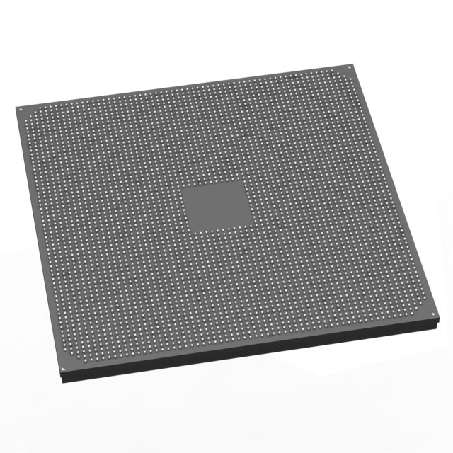
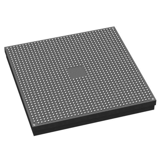
The XCVU19P-2FSVB3824E is a Virtex® UltraScale+™ Field Programmable Gate Array (FPGA) from AMD offered in a 3824-FCBGA surface-mount package. It combines very large programmable logic capacity and significant embedded memory with high I/O density for complex digital designs.
This device provides 8,937,600 logic elements, approximately 79.6 Mbits of embedded memory, and 1,760 I/O pins. Key electrical and environmental data include a supply range of 825 mV to 876 mV, an operating temperature range of 0 °C to 100 °C, extended-grade qualification, and RoHS compliance.
Key Features
- Logic Capacity 8,937,600 logic elements and 510,720 configurable logic blocks to support large-scale programmable designs.
- Embedded Memory Approximately 79.6 Mbits of on-chip RAM for buffering, state storage, and local data handling.
- I/O Density 1,760 I/O pins to support wide external connectivity and multiple parallel interfaces.
- Package & Mounting 3824-FCBGA (65×65) package in a surface-mount form factor for high pin-count, high-density board designs.
- Power Dedicated supply range of 825 mV to 876 mV to guide power-domain design and sequencing.
- Temperature & Grade Extended-grade device rated for operation from 0 °C to 100 °C.
- Compliance RoHS-compliant for environmental and regulatory considerations.
Typical Applications
- High-density FPGA designs — For projects that require very large programmable logic capacity and extensive on-chip memory to implement complex algorithms or large custom compute fabrics.
- High I/O systems — For systems that need broad external connectivity and parallel interfaces, leveraging the device’s 1,760 I/O pins.
- System prototyping and integration — For platform development where a high-pin-count, surface-mount FCBGA package simplifies board-level integration and reduces multi-chip solutions.
Unique Advantages
- Massive programmable logic: 8,937,600 logic elements reduce the need for multiple devices and enable large, consolidated designs.
- Significant embedded memory: Approximately 79.6 Mbits of on-chip RAM provide local storage for buffering, state machines, and data processing.
- Very high I/O count: 1,760 I/O pins simplify external interface design and support dense connectivity requirements.
- Compact, high-pin package: 3824-FCBGA (65×65) surface-mount package enables a compact board footprint while maintaining high signal density.
- Defined power window: 825 mV to 876 mV supply range assists in precise power delivery and design planning.
- Extended operating range: 0 °C to 100 °C rating for applications within that environmental envelope.
Why Choose XCVU19P-2FSVB3824E?
The XCVU19P-2FSVB3824E positions itself as a high-capacity, high-connectivity FPGA suitable for designs that demand extensive programmable logic, substantial on-chip memory, and a large number of I/O. Its 3824-FCBGA surface-mount package and extended-grade rating make it appropriate for complex system-level integrations where board area and signal density are critical.
Choose this device when your project requires consolidating large functions into a single FPGA, maintaining dense external interfacing, and designing within the specified power and temperature ranges. The combination of logic capacity, memory, and I/O provides a scalable platform for advanced digital designs.
Request a quote or submit an inquiry to check pricing and availability for the XCVU19P-2FSVB3824E.


Date Founded: 1969
Headquarters: Santa Clara, California, USA
Employees: 25,000+
Revenue: $22.68 Billion
Certifications and Memberships: ISO9001:2015, RoHS, REACH


