
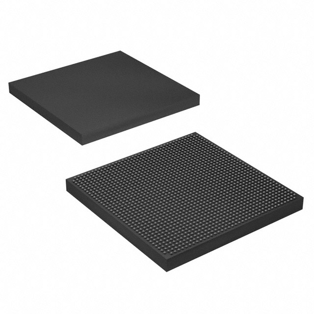
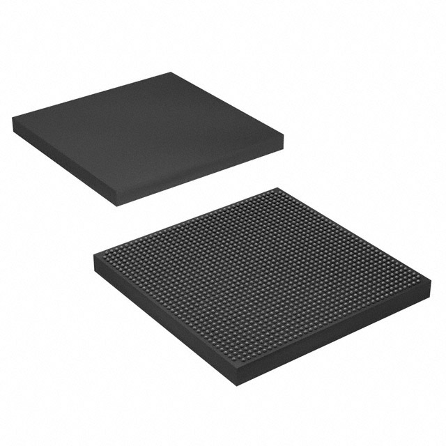
XCVU37P-L2FSVH2892E
| Part Description |
Virtex® UltraScale+™ Field Programmable Gate Array (FPGA) IC 624 74344038 2851800 2892-BBGA, FCBGA |
|---|---|
| Quantity | 275 Available (as of October 8, 2026) |

| Product Category | Field Programmable Gate Array (FPGA) |
|---|---|
| Manufacturer | AMD |
| Manufacturing Status | Last Time Buy |
| Manufacturer Standard Lead Time | 20 Weeks |
| Datasheet |
Specifications & Environmental
| Device Package | 2892-FCBGA (55x55) | Grade | Extended | Operating Temperature | 0°C – 100°C | ||
|---|---|---|---|---|---|---|---|
| Package / Case | 2892-BBGA, FCBGA | Number of I/O | 624 | Voltage | 698 mV - 742 mV | ||
| Mounting Method | Surface Mount | RoHS Compliance | ROHS3 Compliant | REACH Compliance | REACH Unknown | ||
| Moisture Sensitivity Level | 3 (168 Hours) | Number of LABs/CLBs | 162960 | Number of Logic Elements/Cells | 2851800 | ||
| Number of Gates | N/A | ECCN | 3A001A7B | HTS Code | 8542.39.0001 | ||
| Qualification | N/A | Total RAM Bits | 74344038 |
Overview of XCVU37P-L2FSVH2892E – Virtex® UltraScale+™ Field Programmable Gate Array (FPGA) IC
The XCVU37P-L2FSVH2892E is a Virtex® UltraScale+™ FPGA offering a high density of programmable logic and on-chip memory in a 2892-FCBGA (55×55) surface-mount package. It provides approximately 2.85 million logic elements and approximately 74 Mbits of embedded memory, making it suitable for designs that require large amounts of configurable logic and memory resources.
With 624 I/O, an extended-grade temperature rating (0 °C to 100 °C), and a core voltage supply range of 698 mV to 742 mV, this device targets applications that need high integration and significant I/O capacity within a single FPGA package.
Key Features
- Programmable Logic Density Approximately 2,851,800 logic elements provide extensive resources for complex, compute-heavy designs and large-scale programmable functions.
- Embedded Memory Approximately 74 Mbits of on-chip RAM enables memory-intensive logic implementations and reduces the need for external memory components.
- I/O Capacity 624 I/O pins support substantial external interfacing for multi-channel data paths and complex system integration.
- Package and Mounting 2892-FCBGA (55×55) package in a surface-mount format delivers a high-pin-count solution for dense board designs.
- Power Supply Range Core voltage supply specified between 698 mV and 742 mV to match system power-rail requirements.
- Operating Temperature & Grade Extended grade with an operating temperature range of 0 °C to 100 °C for applications requiring broader temperature tolerance than commercial grade.
- RoHS Compliant Meets RoHS requirements for reduced hazardous substances.
Typical Applications
- High-density programmable logic systems Deploys the device's ~2.85M logic elements where large-scale logic implementation and parallel processing are required.
- Memory-intensive designs Leverages approximately 74 Mbits of embedded memory to support complex buffering, look-up tables, and data processing on-chip.
- I/O-rich system integration Uses 624 I/O pins to interface with multiple peripherals, sensors, or multi-lane data streams without immediate reliance on external I/O expanders.
Unique Advantages
- High integration density: Large logic element and embedded memory counts reduce the need for multiple discrete components and simplify board-level architecture.
- Substantial I/O availability: 624 I/O pins enable complex interfacing and broad system connectivity from a single FPGA package.
- Compact, high-pin-count package: 2892-FCBGA (55×55) provides a compact footprint while supporting extensive pinout and signal routing.
- Extended temperature rating: Rated 0 °C to 100 °C to support applications that require a wider operating range than standard commercial-grade devices.
- RoHS compliance: Aligns with environmental regulatory requirements for assembly and deployment.
Why Choose XCVU37P-L2FSVH2892E?
The XCVU37P-L2FSVH2892E is positioned for designs that demand substantial programmable logic, significant on-chip memory, and extensive I/O in a single, surface-mount FCBGA package. Its combination of approximately 2.85 million logic elements, approximately 74 Mbits of embedded RAM, and 624 I/O makes it well suited to integrated systems where consolidation and on-board capability are priorities.
Customers building scalable, high-density FPGA-based systems will find long-term value in the device’s integration level, extended operating range, and RoHS compliance—enabling concise BOMs and simplified board designs while accommodating demanding logic and memory requirements.
Request a quote or submit an inquiry to discuss availability, pricing, and how the XCVU37P-L2FSVH2892E can fit your design requirements.

























Date Founded: 1969
Headquarters: Santa Clara, California, USA
Employees: 25,000+
Revenue: $22.68 Billion
Certifications and Memberships: ISO9001:2015, RoHS, REACH











